- 您现在的位置:买卖IC网 > PDF目录373461 > SN54LVTH540 (Texas Instruments, Inc.) Octal Buffers/Drivers With 3-State Outputs(八缓冲器/驱动器(三态输出)) PDF资料下载
参数资料
| 型号: | SN54LVTH540 |
| 厂商: | Texas Instruments, Inc. |
| 英文描述: | Octal Buffers/Drivers With 3-State Outputs(八缓冲器/驱动器(三态输出)) |
| 中文描述: | 八路缓冲器/驱动器与3态输出(八缓冲器/驱动器(三态输出)) |
| 文件页数: | 1/7页 |
| 文件大小: | 156K |
| 代理商: | SN54LVTH540 |
SN54LVTH540, SN74LVTH540
OCTAL BUFFERS/DRIVERS
WITH 3-STATE OUTPUTS
SCBS681 – MARCH 1997
1
POST OFFICE BOX 655303
DALLAS, TEXAS 75265
State-of-the-Art Advanced BiCMOS
Technology (ABT) Design for 3.3-V
Operation and Low-Static Power
Dissipation
High-Impedance State During Power Up
and Power Down
Bus Hold on Data Inputs Eliminates the
Need for External Pullup/Pulldown
Resistors
Support Mixed-Mode Signal Operation
(5-V Input and Output Voltages With
3.3-V V
CC
)
Support Unregulated Battery Operation
Down to 2.7 V
Typical V
OLP
(Output Ground Bounce)
< 0.8 V at V
CC
= 3.3 V, T
A
= 25
°
C
Power Off Disables Inputs/Outputs,
Permitting Live Insertion
ESD Protection Exceeds 2000 V Per
MIL-STD-883, Method 3015; Exceeds 200 V
Using Machine Model (C = 200 pF, R = 0)
Latch-Up Performance Exceeds 500 mA Per
JESD 17
Package Options Include Plastic
Small-Outline (DW), Shrink Small-Outline
(DB), Thin Shrink Small-Outline (PW), and
Thin Very Small-Outline (DGV) Packages,
Ceramic Chip Carriers (FK), Ceramic Flat
(W) Package, and Ceramic (J) DIPs
description
These octal buffers/drivers are designed specifically for low-voltage (3.3-V) V
CC
operation, but with the
capability to provide a TTL interface to a 5-V system environment.
The ’LVTH540 are ideal for driving bus lines or buffer memory address registers. These devices feature inputs
and outputs on opposite sides of the package that facilitate printed circuit board layout.
The 3-state control gate is a 2-input AND gate with active-low inputs so that if either output-enable (OE1 or OE2)
input is high, all outputs are in the high-impedance state.
Active bus-hold circuitry is provided to hold unused or floating data inputs at a valid logic level.
When V
CC
is between 0 and 1.5 V, the device is in the high-impedance state during power up or power down.
However, to ensure the high-impedance state above 1.5 V, OE should be tied to V
CC
through a pullup resistor;
the minimum value of the resistor is determined by the current-sinking capability of the driver.
The SN54LVTH540 is characterized for operation over the full military temperature range of –55
°
C to 125
°
C.
The SN74LVTH540 is characterized for operation from –40
°
C to 85
°
C.
Copyright
1997, Texas Instruments Incorporated
UNLESS OTHERWISE NOTED this document contains PRODUCTION
DATA information current as of publication date. Products conform to
specifications per the terms of Texas Instruments standard warranty.
Production processing does not necessarily include testing of all
parameters.
Please be aware that an important notice concerning availability, standard warranty, and use in critical applications of
Texas Instruments semiconductor products and disclaimers thereto appears at the end of this data sheet.
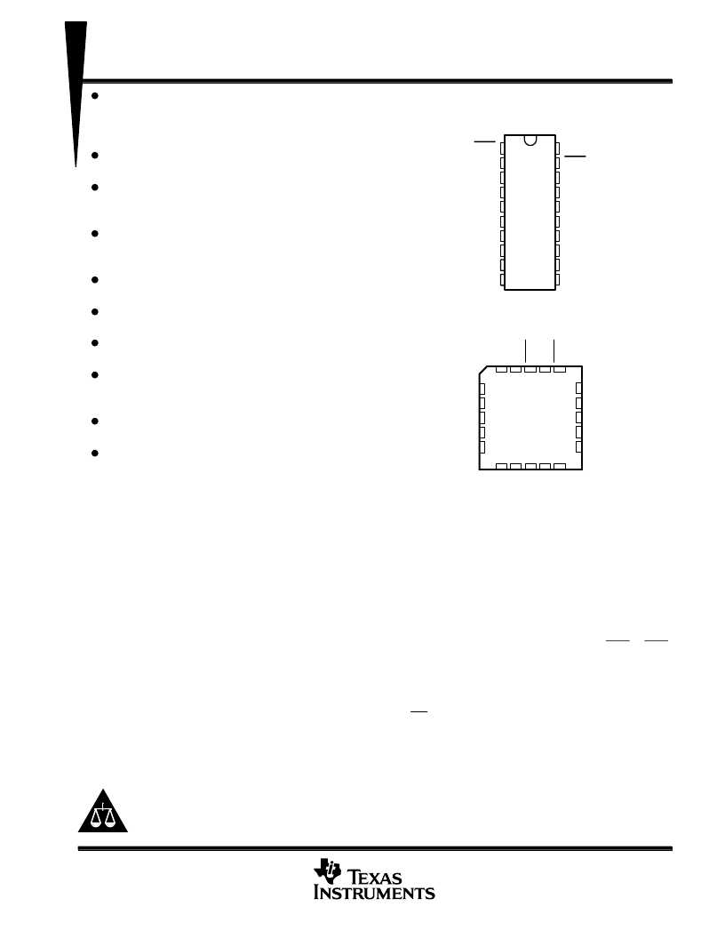
1
2
3
4
5
6
7
8
9
10
20
19
18
17
16
15
14
13
12
11
OE1
A1
A2
A3
A4
A5
A6
A7
A8
GND
V
CC
OE2
Y1
Y2
Y3
Y4
Y5
Y6
Y7
Y8
SN54LVTH540 . . . J OR W PACKAGE
SN74LVTH540 . . . DB, DGV, DW, OR PW PACKAGE
(TOP VIEW)
3
2
1 20 19
9 10 11 12 13
4
5
6
7
8
18
17
16
15
14
Y1
Y2
Y3
Y4
Y5
A3
A4
A5
A6
A7
SN54LVTH540 . . . FK PACKAGE
(TOP VIEW)
A
A
O
Y
Y
O
A
G
Y
V
C
相关PDF资料 |
PDF描述 |
|---|---|
| SN54LVTH541 | Octal Buffers/Drivers With 3-State Outputs(八缓冲器/驱动器(三态输出)) |
| SN54LVTH573FK | Shift Register 3-State; Package: TSSOP-16; No of Pins: 16; Container: Tape and Reel; Qty per Container: 2500 |
| SN54LVTH573J | 3.3-V ABT OCTAL TRANSPARENT D-TYPE LATCHES WITH 3-STATE OUTPUTS |
| SN54LVTH573W | Shift Register 3-State; Package: SOEIAJ-16; No of Pins: 16; Container: Tape and Reel; Qty per Container: 2000 |
| SN74LVTH573DB | 3.3-V ABT OCTAL TRANSPARENT D-TYPE LATCHES WITH 3-STATE OUTPUTS |
相关代理商/技术参数 |
参数描述 |
|---|---|
| SN54S00J | 制造商:Texas Instruments 功能描述:NAND Gate 4-Element 2-IN Bipolar 14-Pin CDIP Tube 制造商:Rochester Electronics LLC 功能描述:- Bulk |
| SN54S00W | 制造商:Rochester Electronics LLC 功能描述:- Bulk |
| SN54S02J | 制造商:Texas Instruments 功能描述: |
| SN54S03J | 制造商:Rochester Electronics LLC 功能描述:- Bulk 制造商:Texas Instruments 功能描述:2-INPUT NAND GATE (OC) - Rail/Tube |
| SN54S04J | 制造商:Texas Instruments 功能描述:Inverter 6-Element Bipolar 14-Pin CDIP Tube 制造商:Rochester Electronics LLC 功能描述:- Bulk 制造商:Texas Instruments 功能描述:INVERTER 6-ELEM BIPOLAR 14CDIP - Rail/Tube 制造商:Texas Instruments 功能描述:HEX INVERTER *NIC* |
发布紧急采购,3分钟左右您将得到回复。