- 您现在的位置:买卖IC网 > PDF目录373464 > SN65HVD3082 (Texas Instruments, Inc.) LOW-POWER RS-485 TRANSCEIVER(低功耗RS-485接口) PDF资料下载
参数资料
| 型号: | SN65HVD3082 |
| 厂商: | Texas Instruments, Inc. |
| 英文描述: | LOW-POWER RS-485 TRANSCEIVER(低功耗RS-485接口) |
| 中文描述: | 低功耗RS - 485收发器(低功耗的RS - 485接口) |
| 文件页数: | 11/14页 |
| 文件大小: | 182K |
| 代理商: | SN65HVD3082 |
SN65HVD3082E
SN75HVD3082E
SLLS562A
–
MARCH 2003
–
REVISED
–
MARCH 2003
www.ti.com
11
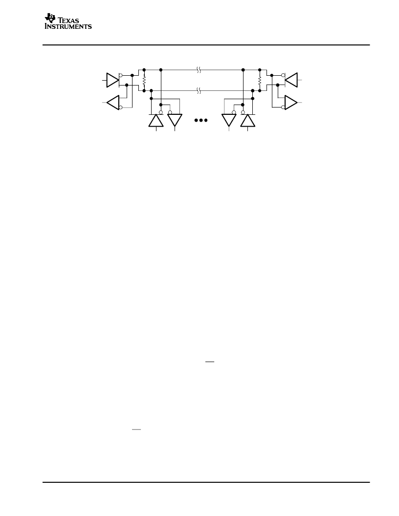
APPLICATION INFORMATION
RT
RT
NOTE:The line should be terminated at both ends with its characteristic impedance (RT = ZO).
Stub lengths off the main line should be kept as short as possible.
Figure 18. Typical Application Circuit
POWER USAGE IN AN RS-485 TRANSCEIVER
Power consumption is a concern in many applications. Power supply current is delivered to the bus load as well as to the
transceiver circuitry. For a typical RS-485 bus configuration, the load that an active driver must drive consists of all of the
receiving nodes, plus the termination resistors at each end of the bus.
The load presented by the receiving nodes depends on the input impedance of the receiver. The TIA/EIA-485-A standard
defines a unit load as allowing up to 1 mA. With up to 32 unit loads allowed on the bus, the total current supplied to all
receivers can be as high as 32 mA. The HVD3082E is rated as a 1/8 unit load device. As shown in Figure 14, the bus input
current is less than 1/8 mA, allowing up to 256 nodes on a single bus.
The current in the termination resistors depends on the differential bus voltage. The standard requires active drivers to
produce at least 1.5 V of differential signal. For a bus terminated with one standard 120-
resistor at each end, this sums
to 25 mA differential output current whenever the bus is active. Typically the HVD3082E can drive more than 25 mA to a
60
load, resulting in a differential output voltage higher than the minimum required by the standard. (See Figure 16.)
Overall, the total load current can be 60 mA to a loaded RS-485 bus. This is in addition to the current required by the
transceiver itself; the HVD3082E circuitry requires only about 0.4 mA with both driver and receiver enabled, and only 0.3
mA with either the driver enabled or with the receiver enabled. In low-power shutdown mode, neither the driver nor receiver
is active, and the supply current is very low.
Supply current increases with signaling rate primarily due to the totum pole outputs of the driver (see Figure 15). When
these outputs change state, there is a moment when both the high-side and low-side output transistors are conducting and
this creates a short spike in the supply current. As the frequency of state changes increases, more power is used.
LOW-POWER SHUTDOWN MODE
When both the driver and receiver are disabled (DE low and RE high) the device is in shutdown mode. If the enable inputs
are in this state for less than 60 ns, the device does not enter shutdown mode. This guards against inadvertently entering
shutdown mode during driver/receiver enabling. Only when the enable inputs are held in this state for 300 ns or more, the
device is assured to be in shutdown mode. In this low-power shutdown mode, most internal circuitry is powered down, and
the supply current is typically 1 nA. When either the driver or the receiver is re-enabled, the internal circuitry becomes active.
If only the driver is re-enabled (DE transitions to high) the driver outputs are driven according to the D input after the enable
times given by t
PZH(SHDN)
and t
PZL(SHDN)
in the driver switching characteristics. If the D input is open when the driver is
enabled, the driver outputs defaults to A high and B low, in accordance with the driver failsafe feature.
If only the receiver is re-enabled (RE transitions to low) the receiver output is driven according to the state of the bus inputs
(A and B) after the enable times given by t
PZH(SHDN)
and t
PZL(SHDN)
in the receiver switching characteristics. If there is no
valid state on the bus the receiver responds as described in the failsafe operation section.
If both the receiver and driver are re-enabled simultaneously, the receiver output is driven according to the state of the bus
inputs (A and B) and the driver output is driven according to the D input. Note that the state of the active driver affects the
inputs to the receiver. Therefore, the receiver outputs are valid as soon as the driver outputs are valid.
相关PDF资料 |
PDF描述 |
|---|---|
| SN65HVD36 | Linear 1-Cell Li-Ion Charger w/Thermal Regulation, 6.5V OVP, Charge Enable 10-SON -40 to 85 |
| SN65HVD36D | Linear 1-Cell Li-Ion Charger w/ Thermal Regulation, 10.5V OVP, Temp Sense 10-SON -40 to 85 |
| SN65HVD38 | Linear 1-Cell Li-Ion Charger w/ Thermal Regulation, 10.5V OVP, Temp Sense 10-SON -40 to 85 |
| SN65HVD38D | Li-Ion Charger with Dynamic Power-Path Management, Output regulated to 4.4V 20-QFN -40 to 85 |
| SN65HVD39 | 3.3V FULL-DUPLEX RS-485 DRIVERS AND RECEIVERS |
相关代理商/技术参数 |
参数描述 |
|---|---|
| SN65HVD3082E | 制造商:TI 制造商全称:Texas Instruments 功能描述:LOW-POWER RS-485 TRANSCEIVER |
| SN65HVD3082E_08 | 制造商:TI 制造商全称:Texas Instruments 功能描述:LOW-POWER RS-485 TRANSCEIVER |
| SN65HVD3082E_09 | 制造商:TI 制造商全称:Texas Instruments 功能描述:Low-Power RS-485 Transceivers, Available in a Small MSOP-8 Package |
| SN65HVD3082E_12 | 制造商:TI 制造商全称:Texas Instruments 功能描述:Low-Power RS-485 Transceivers, Available in a Small MSOP-8Package |
| SN65HVD3082ED | 功能描述:RS-485接口IC LP RS485 RoHS:否 制造商:Texas Instruments 数据速率:250 Kbps 工作电源电压:3.3 V 电源电流:750 uA 工作温度范围:- 40 C to + 125 C 安装风格:SMD/SMT 封装 / 箱体:SOIC-8 封装:Tube |
发布紧急采购,3分钟左右您将得到回复。