- 您现在的位置:买卖IC网 > PDF目录97057 > SN74ABT16825DLG4 (TEXAS INSTRUMENTS INC) ABT SERIES, DUAL 9-BIT DRIVER, TRUE OUTPUT, PDSO56 PDF资料下载
参数资料
| 型号: | SN74ABT16825DLG4 |
| 厂商: | TEXAS INSTRUMENTS INC |
| 元件分类: | 总线收发器 |
| 英文描述: | ABT SERIES, DUAL 9-BIT DRIVER, TRUE OUTPUT, PDSO56 |
| 封装: | GREEN, PLASTIC, SSOP-56 |
| 文件页数: | 4/10页 |
| 文件大小: | 314K |
| 代理商: | SN74ABT16825DLG4 |
SN54ABT16825, SN74ABT16825
18-BIT BUFFERS/DRIVERS
WITH 3-STATE OUTPUTS
SCBS218D – JUNE 1992 – REVISED OCTOBER 2000
3
POST OFFICE BOX 655303
DALLAS, TEXAS 75265
absolute maximum ratings over operating free-air temperature range (unless otherwise noted)
Supply voltage range, VCC
–0.5 V to 7 V
. . . . . . . . . . . . . . . . . . . . . . . . . . . . . . . . . . . . . . . . . . . . . . . . . . . . . . . . . .
Input voltage range, VI (see Note 1)
–0.5 V to 7 V
. . . . . . . . . . . . . . . . . . . . . . . . . . . . . . . . . . . . . . . . . . . . . . . . . .
Voltage range applied to any output in the high or power-off state, VO
–0.5 V to 5.5 V
. . . . . . . . . . . . . . . . . . .
Current into any output in the low state, IO: SN54ABT16825
96 mA
. . . . . . . . . . . . . . . . . . . . . . . . . . . . . . . . . .
SN74ABT16825
128 mA
. . . . . . . . . . . . . . . . . . . . . . . . . . . . . . . . .
Input clamp current, IIK (VI < 0)
–18 mA
. . . . . . . . . . . . . . . . . . . . . . . . . . . . . . . . . . . . . . . . . . . . . . . . . . . . . . . . . . .
Output clamp current, IOK (VO < 0)
–50 mA
. . . . . . . . . . . . . . . . . . . . . . . . . . . . . . . . . . . . . . . . . . . . . . . . . . . . . . . .
Package thermal impedance,
θJA (see Note 2)
56
°C/W
. . . . . . . . . . . . . . . . . . . . . . . . . . . . . . . . . . . . . . . . . . . . .
Storage temperature range, Tstg
–65
°C to 150°C
. . . . . . . . . . . . . . . . . . . . . . . . . . . . . . . . . . . . . . . . . . . . . . . . . . .
Stresses beyond those listed under “absolute maximum ratings” may cause permanent damage to the device. These are stress ratings only, and
functional operation of the device at these or any other conditions beyond those indicated under “recommended operating conditions” is not
implied. Exposure to absolute-maximum-rated conditions for extended periods may affect device reliability.
NOTES:
1. The input and output negative-voltage ratings may be exceeded if the input and output clamp-current ratings are observed.
2. The package thermal impedance is calculated in accordance with JESD 51-7.
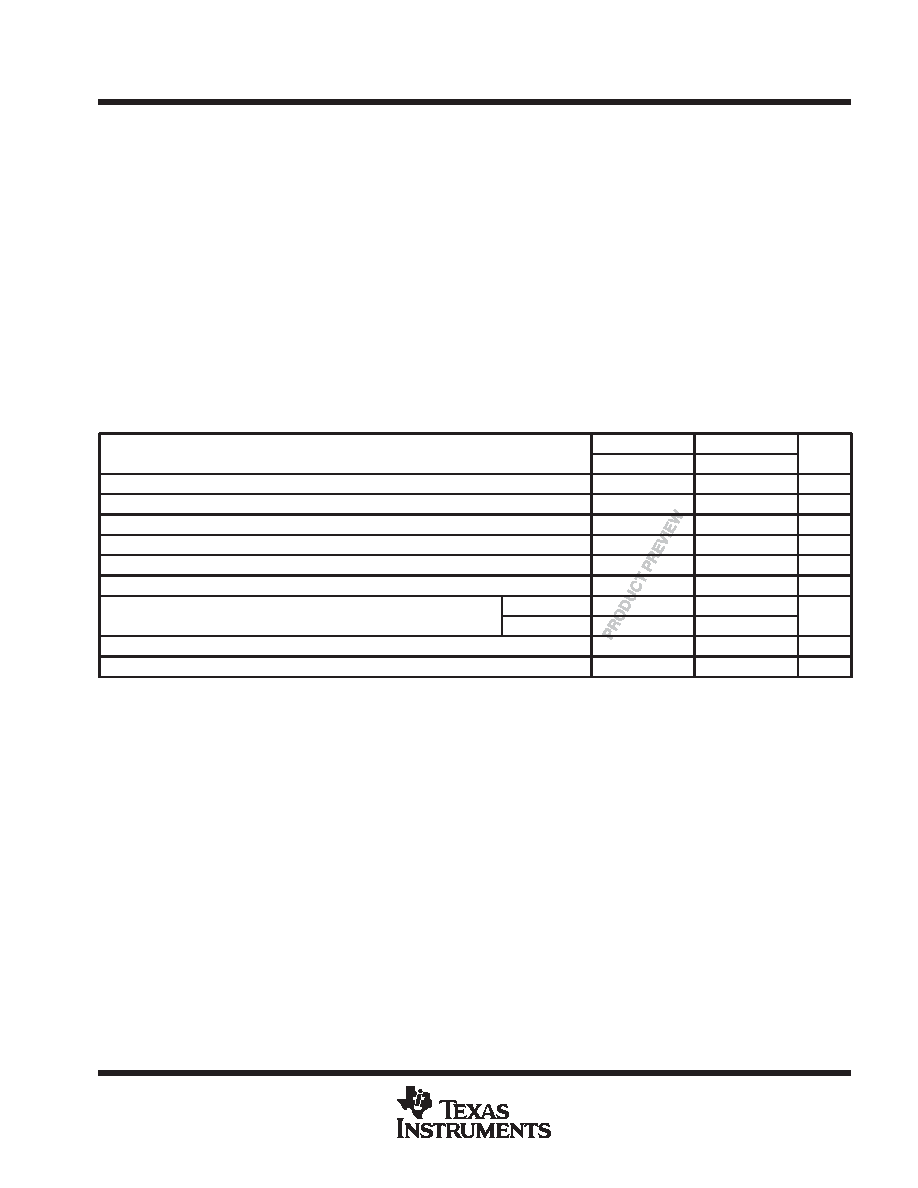
recommended operating conditions (see Note 3)
SN54ABT16825
SN74ABT16825
UNIT
MIN
MAX
MIN
MAX
UNIT
VCC
Supply voltage
4.5
5.5
4.5
5.5
V
VIH
High-level input voltage
2
V
VIL
Low-level input voltage
0.8
V
VI
Input voltage
0
VCC
0
VCC
V
IOH
High-level output current
–24
–32
mA
IOL
Low-level output current
48
64
mA
t/v
Input transition rise or fall rate
Control pins
4
ns/V
t/v
Input transition rise or fall rate
Data pins
10
ns/V
t/VCC
Power-up ramp rate
200
s/V
TA
Operating free-air temperature
–55
125
–40
85
°C
NOTE 3: All unused inputs of the device must be held at VCC or GND to ensure proper device operation. Refer to the TI application report,
Implications of Slow or Floating CMOS Inputs, literature number SCBA004.
PRODUCT PREVIEW information concerns products in the formative or
design phase of development. Characteristic data and other
specifications are design goals. Texas Instruments reserves the right to
change or discontinue these products without notice.
相关PDF资料 |
PDF描述 |
|---|---|
| SN74ABT16827DL | ABT SERIES, DUAL 10-BIT DRIVER, TRUE OUTPUT, PDSO56 |
| SN74ABT16952DGGE4 | ABT SERIES, DUAL 8-BIT REGISTERED TRANSCEIVER, TRUE OUTPUT, PDSO56 |
| SN74ABT2240ADB | ABT SERIES, DUAL 4-BIT DRIVER, INVERTED OUTPUT, PDSO20 |
| SN74ABT2240ADBE4 | ABT SERIES, DUAL 4-BIT DRIVER, INVERTED OUTPUT, PDSO20 |
| SN74ABT2244DBR | ABT SERIES, DUAL 4-BIT DRIVER, TRUE OUTPUT, PDSO20 |
相关代理商/技术参数 |
参数描述 |
|---|---|
| SN74ABT16825DLR | 功能描述:缓冲器和线路驱动器 Tri-State 18-Bit RoHS:否 制造商:Micrel 输入线路数量:1 输出线路数量:2 极性:Non-Inverting 电源电压-最大:+/- 5.5 V 电源电压-最小:+/- 2.37 V 最大工作温度:+ 85 C 安装风格:SMD/SMT 封装 / 箱体:MSOP-8 封装:Reel |
| SN74ABT16825DLRG4 | 功能描述:缓冲器和线路驱动器 18-Bit Buffer/Driver With 3-State Outputs RoHS:否 制造商:Micrel 输入线路数量:1 输出线路数量:2 极性:Non-Inverting 电源电压-最大:+/- 5.5 V 电源电压-最小:+/- 2.37 V 最大工作温度:+ 85 C 安装风格:SMD/SMT 封装 / 箱体:MSOP-8 封装:Reel |
| SN74ABT16827 | 制造商:TI 制造商全称:Texas Instruments 功能描述:20-BIT BUFFERS/DRIVERS WITH 3-STATE OUTPUTS |
| SN74ABT16827DGGR | 制造商:Rochester Electronics LLC 功能描述:- Bulk |
| SN74ABT16827DL | 功能描述:缓冲器和线路驱动器 20-Bit Buffer/Driver With 3-State Outputs RoHS:否 制造商:Micrel 输入线路数量:1 输出线路数量:2 极性:Non-Inverting 电源电压-最大:+/- 5.5 V 电源电压-最小:+/- 2.37 V 最大工作温度:+ 85 C 安装风格:SMD/SMT 封装 / 箱体:MSOP-8 封装:Reel |
发布紧急采购,3分钟左右您将得到回复。