- 您现在的位置:买卖IC网 > PDF目录97059 > SN74ALS114AD (TEXAS INSTRUMENTS INC) ALS SERIES, DUAL NEGATIVE EDGE TRIGGERED J-K FLIP-FLOP, COMPLEMENTARY OUTPUT, PDSO14 PDF资料下载
参数资料
| 型号: | SN74ALS114AD |
| 厂商: | TEXAS INSTRUMENTS INC |
| 元件分类: | 锁存器 |
| 英文描述: | ALS SERIES, DUAL NEGATIVE EDGE TRIGGERED J-K FLIP-FLOP, COMPLEMENTARY OUTPUT, PDSO14 |
| 封装: | PLASTIC, SOIC-14 |
| 文件页数: | 1/4页 |
| 文件大小: | 70K |
| 代理商: | SN74ALS114AD |
SN54ALS114A, SN74ALS114A
DUAL JK NEGATIVEEDGETRIGGERED FLIPFLOPS
WITH PRESET,COMMON CLEAR,AND COMMON CLOCK
SDAS201 D2661, DECEMBER 1982 REVISED MAY 1986
POST OFFICE BOX 655303
DALLAS, TEXAS 75265
POST OFFICE BOX 1443
HOUSTON, TEXAS 77001
Copyright
1986, Texas Instruments Incorporated
5BASIC
1
Fully Buffered to Offer Maximum isolation
from External Disturbance
Package Options include Plastic Small
Outline Packages, Ceramic Chip Carriers,
and Standard Plastic and Ceramic 300-mil
DIPs
Typical Maximum Clock Frequency
30 MHz
Typical Power Dissipation per Flip-Flop
6 mW
Dependable Texas Instruments Quality and
Reliability
description
These devices contain two independent J-K
negative-edge-triggered flip-flops. A low level at
the Preset or Clear inputs sets or resets the
outputs regardless of the levels of the other inputs.
When Preset and Clear are inactive (high), data at
the J and K inputs meeting the setup time
requirements are transferred to the outputs on the
negative-going edge of the clock pulse. Clock
triggering occurs at a voltage level and is not
directly related to the fall time of the clock pulse.
Following the hold time interval, data at the J and
K inputs may be changed without affecting the
levels at the outputs. These versatile flip-flops can
perform as toggle flip-flops by tying J and K high.
The SN54ALS114A is characterized for operation
over the full military temperature range of 55
°C
to 125
°C. The SN74ALS114A is characterized for
operation from 0
°C to 70°C.
FUNCTION TABLE
INPUTS
OUTPUTS
PRE
CLR
CLK
J
K
Q
L
H
X
H
L
H
LX
X
L
H
L
X
XXH
H
↓
LL
Q0
H
↓
HL
H
L
H
↓
LH
L
H
↓
H
TOGGLE
H
X
Q0
The output levels in this configuration are not guaranteed to
meet the minimum levels for VOH if the lows at Preset and
Clear are near VIL maximum. Furthermore, this configuration
is nonstable; that is, it will not persist when either Preset or
Clear returns to its inactive (high) level.
logic symbol
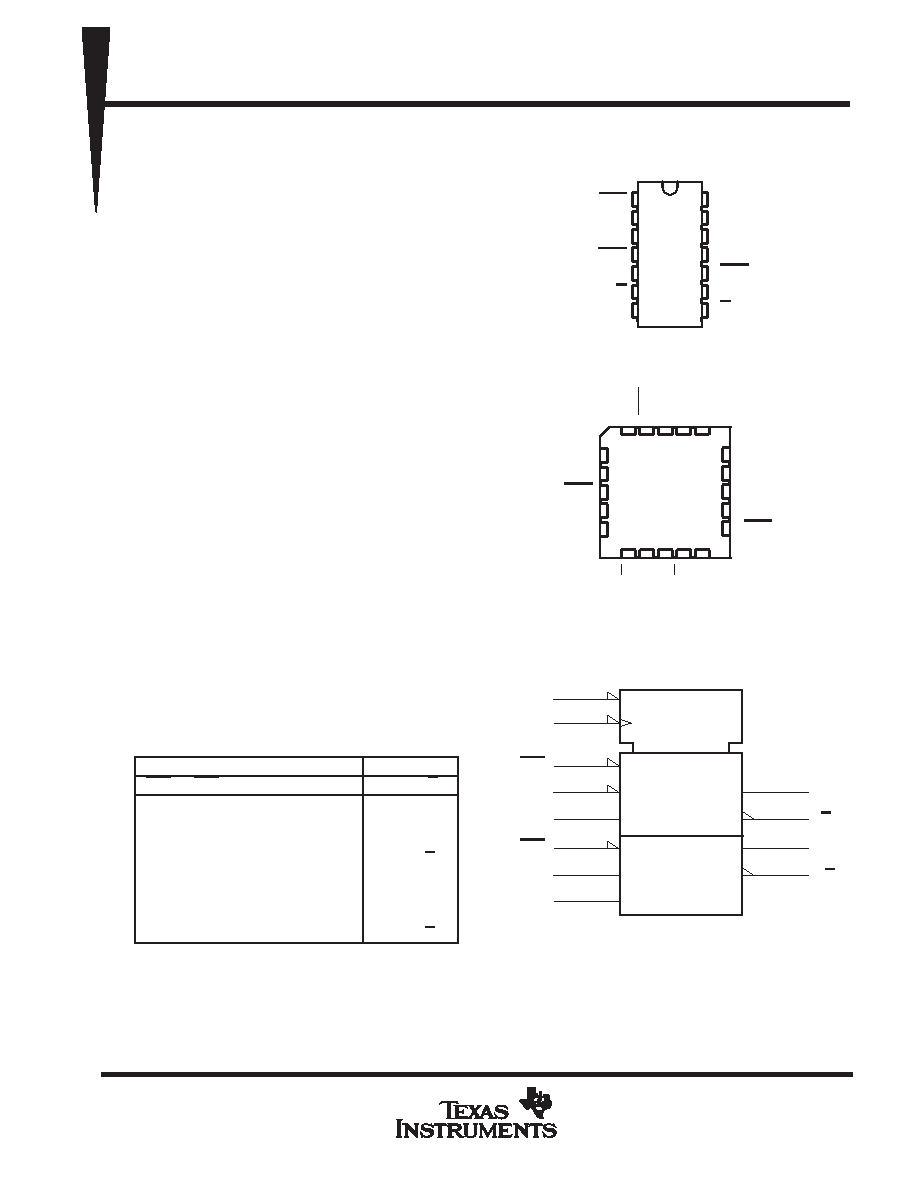
Pin numbers are for D, J, and N packages.
1Q
2Q
8
9
6
5
R
1K
C1
1J
S
12
2K
10
2PRE
13
CLK
11
2J
2
1K
1
CLR
3
1J
1PRE
4
1
2
3
4
5
6
7
14
13
12
11
10
9
8
CLR
1K
1J
1PRE
1Q
GND
VCC
CLK
2K
2J
2PRE
2Q
SN54ALS114A ...J PACKAGE
SN74ALS114A ...D OR N PACKAGE
(TOP VIEW)
3
2
1 20 19
910 11 12 13
4
5
6
7
8
18
17
16
15
14
2K
NC
2J
NC
2PRE
1J
NC
1PRE
NC
1Q
SN54ALS114A . . . FK PACKAGE
(TOP VIEW)
1K
1CLR
NC
2Q
CLK
1Q
GND
NC
V
CC
NCNo internal connection
This symbol is in accordance with ANSI/IEEE Std 911-1984 and
IEC Publication 617-12.
PRODUCTION DATA information is current as of publication date.
Products conform to specifications per the terms of Texas Instruments
standard warranty. Production processing does not necessarily include
testing of all parameters.
相关PDF资料 |
PDF描述 |
|---|---|
| SN74ALS1242N3 | ALS SERIES, 4-BIT TRANSCEIVER, INVERTED OUTPUT, PDIP14 |
| SN74ALS1245FN-00 | ALS SERIES, 8-BIT TRANSCEIVER, TRUE OUTPUT, PQCC20 |
| SN74ALS137DR | ALS SERIES, OTHER DECODER/DRIVER, INVERTED OUTPUT, PDSO16 |
| SN74AS137N3 | AS SERIES, OTHER DECODER/DRIVER, INVERTED OUTPUT, PDIP16 |
| SN74ALS138N3 | ALS SERIES, OTHER DECODER/DRIVER, INVERTED OUTPUT, PDIP16 |
相关代理商/技术参数 |
参数描述 |
|---|---|
| SN74ALS11AD | 功能描述:逻辑门 Triple 3-Input Positive-NAND Gate RoHS:否 制造商:Texas Instruments 产品:OR 逻辑系列:LVC 栅极数量:2 线路数量(输入/输出):2 / 1 高电平输出电流:- 16 mA 低电平输出电流:16 mA 传播延迟时间:3.8 ns 电源电压-最大:5.5 V 电源电压-最小:1.65 V 最大工作温度:+ 125 C 安装风格:SMD/SMT 封装 / 箱体:DCU-8 封装:Reel |
| SN74ALS11ADE4 | 功能描述:逻辑门 Triple 3-Input Positive-NAND Gate RoHS:否 制造商:Texas Instruments 产品:OR 逻辑系列:LVC 栅极数量:2 线路数量(输入/输出):2 / 1 高电平输出电流:- 16 mA 低电平输出电流:16 mA 传播延迟时间:3.8 ns 电源电压-最大:5.5 V 电源电压-最小:1.65 V 最大工作温度:+ 125 C 安装风格:SMD/SMT 封装 / 箱体:DCU-8 封装:Reel |
| SN74ALS11ADG4 | 功能描述:逻辑门 Triple 3 Inpt Pos AND Gates RoHS:否 制造商:Texas Instruments 产品:OR 逻辑系列:LVC 栅极数量:2 线路数量(输入/输出):2 / 1 高电平输出电流:- 16 mA 低电平输出电流:16 mA 传播延迟时间:3.8 ns 电源电压-最大:5.5 V 电源电压-最小:1.65 V 最大工作温度:+ 125 C 安装风格:SMD/SMT 封装 / 箱体:DCU-8 封装:Reel |
| SN74ALS11ADR | 功能描述:逻辑门 Triple 3-Input RoHS:否 制造商:Texas Instruments 产品:OR 逻辑系列:LVC 栅极数量:2 线路数量(输入/输出):2 / 1 高电平输出电流:- 16 mA 低电平输出电流:16 mA 传播延迟时间:3.8 ns 电源电压-最大:5.5 V 电源电压-最小:1.65 V 最大工作温度:+ 125 C 安装风格:SMD/SMT 封装 / 箱体:DCU-8 封装:Reel |
| SN74ALS11ADRE4 | 功能描述:逻辑门 Triple 3-Input Positive-NAND Gate RoHS:否 制造商:Texas Instruments 产品:OR 逻辑系列:LVC 栅极数量:2 线路数量(输入/输出):2 / 1 高电平输出电流:- 16 mA 低电平输出电流:16 mA 传播延迟时间:3.8 ns 电源电压-最大:5.5 V 电源电压-最小:1.65 V 最大工作温度:+ 125 C 安装风格:SMD/SMT 封装 / 箱体:DCU-8 封装:Reel |
发布紧急采购,3分钟左右您将得到回复。