- 您现在的位置:买卖IC网 > PDF目录98101 > SN74ALS805ANE4 (TEXAS INSTRUMENTS INC) ALS SERIES, HEX 2-INPUT NOR GATE, PDIP20 PDF资料下载
参数资料
| 型号: | SN74ALS805ANE4 |
| 厂商: | TEXAS INSTRUMENTS INC |
| 元件分类: | 门电路 |
| 英文描述: | ALS SERIES, HEX 2-INPUT NOR GATE, PDIP20 |
| 封装: | 0.300 INCH, PLASTIC, DIP-20 |
| 文件页数: | 1/15页 |
| 文件大小: | 584K |
| 代理商: | SN74ALS805ANE4 |
SN54ALS805A, SN54AS805B, SN74ALS805A, SN74AS805B
HEX 2INPUT NOR DRIVERS
SDAS023C DECEMBER 1982 REVISED JANUARY 1995
Copyright
1995, Texas Instruments Incorporated
1
POST OFFICE BOX 655303
DALLAS, TEXAS 75265
POST OFFICE BOX 1443
HOUSTON, TEXAS 772511443
High Capacitive-Drive Capability
′ALS805A Has Typical Delay Time of 4.2 ns
(CL = 50 pF) and Typical Power Dissipation
of 4.2 mW Per Gate
′AS805B Has Typical Delay Time of 2.6 ns
(CL = 50 pF) and Typical Power Dissipation
of 12 mW Per Gate
Package Options Include Plastic
Small-Outline (DW) Packages, Ceramic
Chip Carriers (FK), and Standard Plastic (N)
and Ceramic (J) 300-mil DIPs
description
These devices contain six independent 2-input
NOR drivers. They perform the Boolean functions
Y = A + B or Y = A
B in positive logic.
The
SN54ALS805A
and
SN54AS805B
are
characterized for operation over the full military
temperature range of 55
°C to 125°C. The
SN74ALS805A
and
SN74AS805B
are
characterized for operation from 0
°C to 70°C.
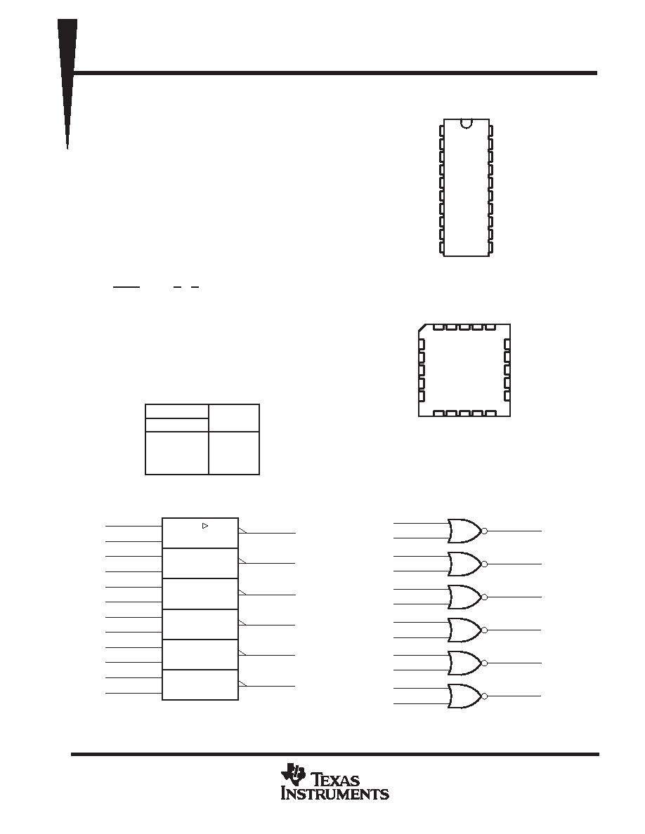
FUNCTION TABLE
(each driver)
INPUTS
OUTPUT
A
B
OUTPUT
Y
H
X
L
X
HL
L
H
logic symbol
logic diagram (positive logic)
1
1A
2
1B
4
2A
5
2B
7
3A
8
3B
12
4A
13
4B
1Y
3
2Y
6
3Y
9
4Y
11
15
5A
16
5B
18
6A
19
6B
5Y
14
6Y
17
1Y
3
2Y
6
3Y
9
4Y
11
5Y
14
6Y
17
≥1
1
1A
2
1B
4
2A
5
2B
7
3A
8
3B
12
4A
13
4B
15
5A
16
5B
18
6A
19
6B
This symbol is in accordance with ANSI/IEEE Std 91-1984 and
IEC Publication 617-12.
1
2
3
4
5
6
7
8
9
10
20
19
18
17
16
15
14
13
12
11
1A
1B
1Y
2A
2B
2Y
3A
3B
3Y
GND
VCC
6B
6A
6Y
5B
5A
5Y
4B
4A
4Y
SN54ALS805A, SN54AS805B...J PACKAGE
SN74ALS805A, SN74AS805B...DW OR N PACKAGE
(TOP VIEW)
3
2
1 20 19
910 11 12 13
4
5
6
7
8
18
17
16
15
14
6A
6Y
5B
5A
5Y
2A
2B
2Y
3A
3B
SN54ALS805A, SN54AS805B...FK PACKAGE
(TOP VIEW)
1Y
1B
1A
4A
4B
6B
3Y
G
ND
4Y
V
CC
PRODUCTION DATA information is current as of publication date.
Products conform to specifications per the terms of Texas Instruments
standard warranty. Production processing does not necessarily include
testing of all parameters.
相关PDF资料 |
PDF描述 |
|---|---|
| SN74AS805BDWRG4 | AS SERIES, HEX 2-INPUT NOR GATE, PDSO20 |
| SN74ALS819DWR | ALS SERIES, 8-BIT DRIVER, TRUE OUTPUT, PDSO24 |
| SN74ALS832ADWRE4 | ALS SERIES, HEX 2-INPUT OR GATE, PDSO20 |
| SN74ALS869DWR | ALS SERIES, SYN POSITIVE EDGE TRIGGERED 8-BIT BIDIRECTIONAL BINARY COUNTER, PDSO24 |
| SN74ALS869NT | ALS SERIES, SYN POSITIVE EDGE TRIGGERED 8-BIT BIDIRECTIONAL BINARY COUNTER, PDIP24 |
相关代理商/技术参数 |
参数描述 |
|---|---|
| SN74ALS805FN | 制造商:. 功能描述: |
| SN74ALS808AFN | 制造商:Rochester Electronics LLC 功能描述:- Bulk 制造商:Texas Instruments 功能描述: |
| SN74ALS808FN | 制造商:. 功能描述: |
| SN74ALS810N | 制造商:Rochester Electronics LLC 功能描述:- Bulk |
| SN74ALS812NT | 制造商:Rochester Electronics LLC 功能描述:- Tape and Reel |
发布紧急采购,3分钟左右您将得到回复。