- 您现在的位置:买卖IC网 > PDF目录98107 > SN74AUP1G79DSFR (TEXAS INSTRUMENTS INC) AUP/ULP/V SERIES, POSITIVE EDGE TRIGGERED D FLIP-FLOP, TRUE OUTPUT, PDSO6 PDF资料下载
参数资料
| 型号: | SN74AUP1G79DSFR |
| 厂商: | TEXAS INSTRUMENTS INC |
| 元件分类: | 锁存器 |
| 英文描述: | AUP/ULP/V SERIES, POSITIVE EDGE TRIGGERED D FLIP-FLOP, TRUE OUTPUT, PDSO6 |
| 封装: | GREEN, PLASTIC, MO-287X2AAF, SON-6 |
| 文件页数: | 1/27页 |
| 文件大小: | 1158K |
| 代理商: | SN74AUP1G79DSFR |
当前第1页第2页第3页第4页第5页第6页第7页第8页第9页第10页第11页第12页第13页第14页第15页第16页第17页第18页第19页第20页第21页第22页第23页第24页第25页第26页第27页
3
2
4
5
1
D
V
CC
Q
CLK
GND
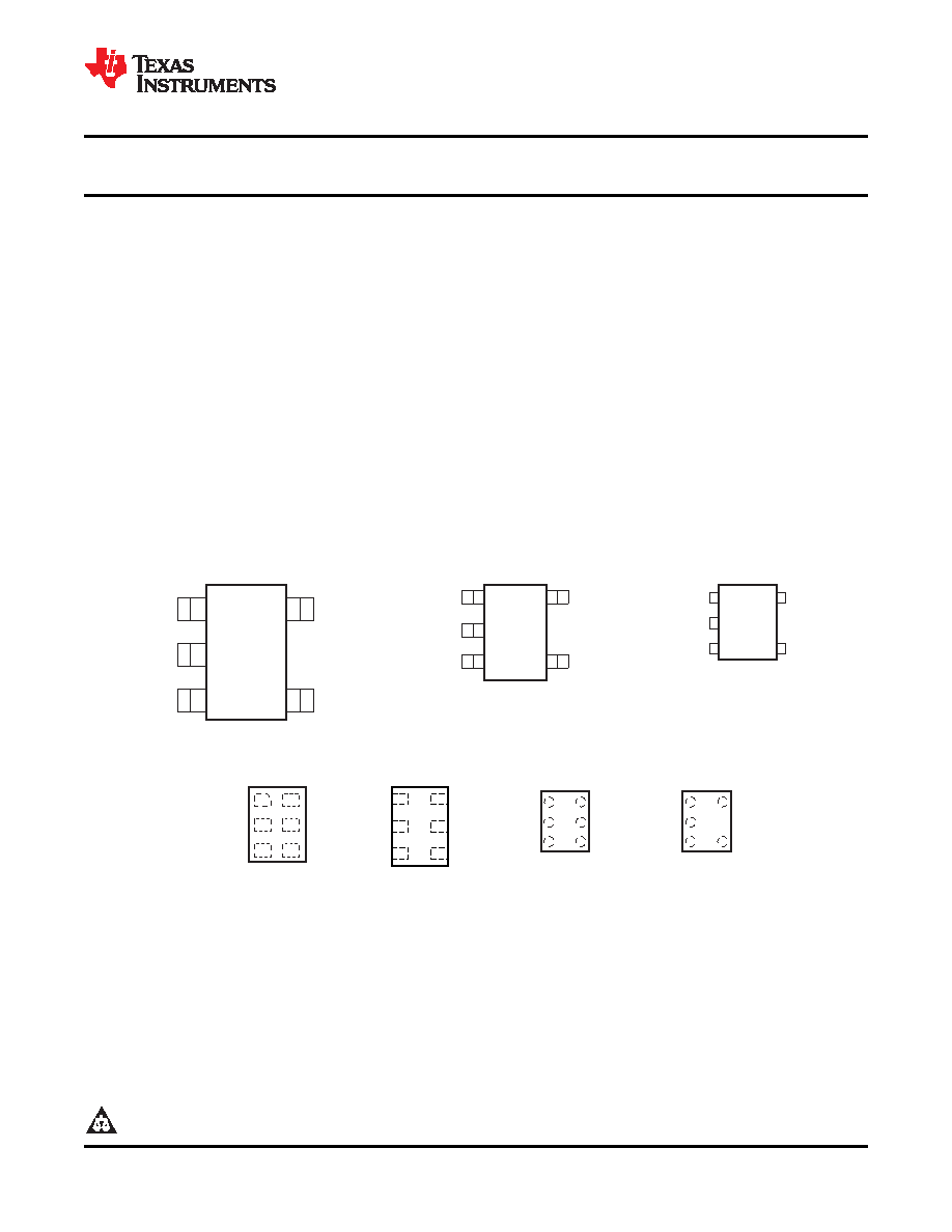
DCK PACKAGE
(TOP VIEW)
3
2
4
5
1
D
V
CC
Q
CLK
GND
DRL PACKAGE
(TOP VIEW)
DBV PACKAGE
(TOP VIEW)
3
2
4
5
1
D
V
CC
Q
CLK
GND
DRY PACKAGE
(TOP VIEW)
CLK
N.C.
D
6
5
4
2
3
GND
Q
V
CC
1
GND
Q
3
4
CLK
2
5
D
6
1
N.C.
V
CC
DSF PACKAGE
(TOP VIEW)
YZP PACKAGE
(TOP VIEW)
GND
D
Q
V
CC
CLK
3
5
2
1
4
A1
B1
C1
A2
C2
YFP PACKAGE
(TOP VIEW)
GND
D
Q
V
CC
CLK
3
6
2
1
4
5
N.C.
A1
B1
C1
A2
B2
C2
www.ti.com
SCES592G – JULY 2004 – REVISED MAY 2010
LOW-POWER SINGLE POSITIVE-EDGE-TRIGGERED D-TYPE FLIP-FLOP
Check for Samples: SN74AUP1G79
1
FEATURES
Available in the Texas Instruments NanoStar
Wide Operating VCC Range of 0.8 V to 3.6 V
Package
Optimized for 3.3-V Operation
Low Static-Power Consumption:
3.6-V I/O Tolerant to Support Mixed-Mode
ICC = 0.9 mA Max
Signal Operation
Low Dynamic-Power Consumption:
tpd = 4 ns Max at 3.3 V
Cpd = 3 pF Typ at 3.3 V
Suitable for Point-to-Point Applications
Low Input Capacitance:
Latch-Up Performance Exceeds 100 mA Per
Ci = 1.5 pF Typ
JESD 78, Class II
Low Noise: Overshoot and Undershoot
ESD Performance Tested Per JESD 22
<10% of VCC
–
2000-V Human-Body Model
Ioff Supports Partial Power-Down-Mode
(A114-B, Class II)
Operation
–
1000-V Charged-Device Model (C101)
Input Hysteresis Allows Slow Input Transition
and Better Switching Noise Immunity at the
Input (Vhys = 250 mV Typ at 3.3 V)
N.C. – No internal connection
See mechanical drawings for dimensions.
DESCRIPTION/ORDERING INFORMATION
The AUP family is TI's premier solution to the industry's low-power needs in battery-powered portable
applications. This family ensures a very low static and dynamic power consumption across the entire VCC range
of 0.8 V to 3.6 V, resulting in an increased battery life. This product also maintains excellent signal integrity (see
Figure 1 and Figure 2).
1
Please be aware that an important notice concerning availability, standard warranty, and use in critical applications of Texas
Instruments semiconductor products and disclaimers thereto appears at the end of this data sheet.
PRODUCTION DATA information is current as of publication date.
Copyright 2004–2010, Texas Instruments Incorporated
Products conform to specifications per the terms of the Texas
Instruments standard warranty. Production processing does not
necessarily include testing of all parameters.
相关PDF资料 |
PDF描述 |
|---|---|
| SN74AUP1G80DBVRE4 | AUP/ULP/V SERIES, POSITIVE EDGE TRIGGERED D FLIP-FLOP, INVERTED OUTPUT, PDSO5 |
| SN74AUP1G98YZPR | SPECIALTY LOGIC CIRCUIT, BGA6 |
| SN74AUP1G98DCKTG4 | SPECIALTY LOGIC CIRCUIT, PDSO6 |
| SN74AUP1G99DCUT | SPECIALTY LOGIC CIRCUIT, PDSO8 |
| SN74AUP1T02DCKT | AUP/ULP/V SERIES, 2-INPUT NOR GATE, PDSO5 |
相关代理商/技术参数 |
参数描述 |
|---|---|
| SN74AUP1G79YFPR | 功能描述:触发器 Low-Pwr Sgl Pos-Edge Trgrd D-Type RoHS:否 制造商:Texas Instruments 电路数量:2 逻辑系列:SN74 逻辑类型:D-Type Flip-Flop 极性:Inverting, Non-Inverting 输入类型:CMOS 输出类型: 传播延迟时间:4.4 ns 高电平输出电流:- 16 mA 低电平输出电流:16 mA 电源电压-最大:5.5 V 最大工作温度:+ 85 C 安装风格:SMD/SMT 封装 / 箱体:X2SON-8 封装:Reel |
| SN74AUP1G79YZPR | 功能描述:触发器 LoPwrSngl+EdgeTrggrd DTypeFlipFlop RoHS:否 制造商:Texas Instruments 电路数量:2 逻辑系列:SN74 逻辑类型:D-Type Flip-Flop 极性:Inverting, Non-Inverting 输入类型:CMOS 输出类型: 传播延迟时间:4.4 ns 高电平输出电流:- 16 mA 低电平输出电流:16 mA 电源电压-最大:5.5 V 最大工作温度:+ 85 C 安装风格:SMD/SMT 封装 / 箱体:X2SON-8 封装:Reel |
| SN74AUP1G80DBVR | 功能描述:触发器 LoPwrSngl+Pos Edge Trggrd DType RoHS:否 制造商:Texas Instruments 电路数量:2 逻辑系列:SN74 逻辑类型:D-Type Flip-Flop 极性:Inverting, Non-Inverting 输入类型:CMOS 输出类型: 传播延迟时间:4.4 ns 高电平输出电流:- 16 mA 低电平输出电流:16 mA 电源电压-最大:5.5 V 最大工作温度:+ 85 C 安装风格:SMD/SMT 封装 / 箱体:X2SON-8 封装:Reel |
| SN74AUP1G80DBVRE4 | 功能描述:触发器 Lo PWR SNGL Pos Edge Trgrd DType FlipFlop RoHS:否 制造商:Texas Instruments 电路数量:2 逻辑系列:SN74 逻辑类型:D-Type Flip-Flop 极性:Inverting, Non-Inverting 输入类型:CMOS 输出类型: 传播延迟时间:4.4 ns 高电平输出电流:- 16 mA 低电平输出电流:16 mA 电源电压-最大:5.5 V 最大工作温度:+ 85 C 安装风格:SMD/SMT 封装 / 箱体:X2SON-8 封装:Reel |
| SN74AUP1G80DBVRG4 | 功能描述:触发器 Lo PWR SNGL Pos Edge Trgrd DType FlipFlop RoHS:否 制造商:Texas Instruments 电路数量:2 逻辑系列:SN74 逻辑类型:D-Type Flip-Flop 极性:Inverting, Non-Inverting 输入类型:CMOS 输出类型: 传播延迟时间:4.4 ns 高电平输出电流:- 16 mA 低电平输出电流:16 mA 电源电压-最大:5.5 V 最大工作温度:+ 85 C 安装风格:SMD/SMT 封装 / 箱体:X2SON-8 封装:Reel |
发布紧急采购,3分钟左右您将得到回复。