- 您现在的位置:买卖IC网 > PDF目录225203 > SN74AUP1G99YEPR (TEXAS INSTRUMENTS INC) SPECIALTY LOGIC CIRCUIT, PBGA8 PDF资料下载
参数资料
| 型号: | SN74AUP1G99YEPR |
| 厂商: | TEXAS INSTRUMENTS INC |
| 元件分类: | 标准逻辑 |
| 英文描述: | SPECIALTY LOGIC CIRCUIT, PBGA8 |
| 封装: | DSBGA-8 |
| 文件页数: | 1/24页 |
| 文件大小: | 413K |
| 代理商: | SN74AUP1G99YEPR |
www.ti.com
FEATURES
D
3
2
5
8
1
OE
VCC
A
GND
DCT PACKAGE
(TOP VIEW)
YEP OR YZP PACKAGE
(BOTTOM VIEW)
DCU PACKAGE
(TOP VIEW)
3
2
4
5
1
OE
VCC
Y
A
GND
A
GND
VCC
C
B
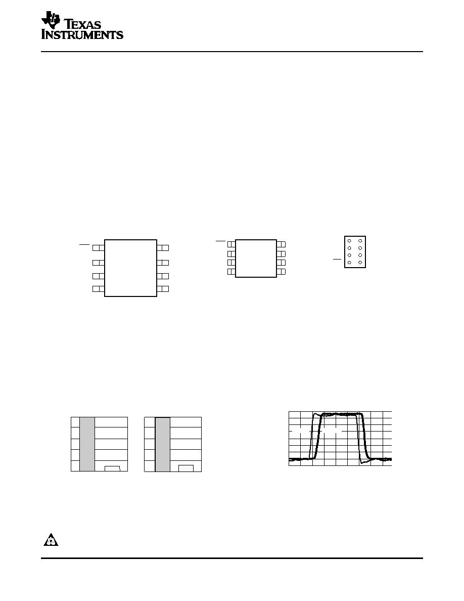
See mechanical drawings for dimensions.
2
5
3
4
8
B
D
C
B
Y
C
4
6
7
6
7
8
6
1
7
OE
D
Y
DESCRIPTION/ORDERING INFORMATION
AUP
LVC
AUP
LVC
Static-Power Consumption
(
A)
Dynamic-Power Consumption
(pF)
Single, dual, and triple gates
3.3-V
Logic
3.3-V
Logic
0%
20%
40%
60%
80%
100%
0%
20%
40%
60%
80%
100%
0.5
0
0.5
1
1.5
2
2.5
3
3.5
0
5
10
15
20
25
30
35
40
45
Time ns
V
oltage
V
AUP1G08 data at C
L = 15 pF
Switching Characteristics
at 25 MHz
Output
Input
SN74AUP1G99
LOW-POWER ULTRA-CONFIGURABLE MULTIPLE-FUNCTION GATE
WITH 3-STATE OUTPUTS
SCES594B – JULY 2004 – REVISED AUGUST 2005
Available in the Texas Instruments
Wide Operating V
CC Range of 0.8 V to 3.6 V
NanoStar and NanoFree Packages
Optimized for 3.3-V Operation
Low Static-Power Consumption
3.6-V I/O Tolerant to Support Mixed-Mode
(I
CC = 0.9 A Max)
Signal Operation
Low Dynamic-Power Consumption
t
pd = 7.4 ns Max at 3.3 V
(C
pd = 5 pF Typ at 3.3 V)
Suitable for Point-to-Point Applications
Low Input Capacitance (C
i = 1.5 pF)
Latch-Up Performance Exceeds 100 mA Per
Low Noise – Overshoot and Undershoot
JESD 78, Class II
<10% of V
CC
ESD Performance Tested Per JESD 22
Input-Disable Feature Allows Floating Input
– 2000-V Human-Body Model
Conditions
(A114-B, Class II)
I
off Supports Partial-Power-Down Mode
– 200-V Machine Model (A115-A)
Operation
– 1000-V Charged-Device Model (C101)
Includes Schmitt-Trigger Inputs
The AUP family is TI's premier solution to the industry's low-power needs in battery-powered portable
applications. This family ensures a very low static- and dynamic-power consumption across the entire VCC range
of 0.8 V to 3.6 V, resulting in an increased battery life. This product also maintains excellent signal integrity (see
Figures 1 and 2).
xxxxxx
Figure 1. AUP - The Lowest-Power Family
Figure 2. Excellent Signal Integrity
Please be aware that an important notice concerning availability, standard warranty, and use in critical applications of Texas
Instruments semiconductor products and disclaimers thereto appears at the end of this data sheet.
NanoStar, NanoFree are trademarks of Texas Instruments.
PRODUCTION DATA information is current as of publication date.
Copyright 2004–2005, Texas Instruments Incorporated
Products conform to specifications per the terms of the Texas
Instruments standard warranty. Production processing does not
necessarily include testing of all parameters.
相关PDF资料 |
PDF描述 |
|---|---|
| SN74BCT241DWE4 | BCT/FBT SERIES, DUAL 4-BIT DRIVER, TRUE OUTPUT, PDSO20 |
| SN74CBTD1G125DCKR | CBT/FST/QS/5C/B SERIES, 1-BIT DRIVER, TRUE OUTPUT, PDSO5 |
| SN74HC03NE4 | HC/UH SERIES, QUAD 2-INPUT NAND GATE, PDIP14 |
| SN74HC27DRE4 | HC/UH SERIES, TRIPLE 3-INPUT NOR GATE, PDSO14 |
| SN74HC7002PWRG4 | HC/UH SERIES, QUAD 2-INPUT NOR GATE, PDSO14 |
相关代理商/技术参数 |
参数描述 |
|---|---|
| SN74AUP1G99YZPR | 功能描述:逻辑门 LoPwr Ultra Conf MultFunctionGt RoHS:否 制造商:Texas Instruments 产品:OR 逻辑系列:LVC 栅极数量:2 线路数量(输入/输出):2 / 1 高电平输出电流:- 16 mA 低电平输出电流:16 mA 传播延迟时间:3.8 ns 电源电压-最大:5.5 V 电源电压-最小:1.65 V 最大工作温度:+ 125 C 安装风格:SMD/SMT 封装 / 箱体:DCU-8 封装:Reel |
| SN74AUP1GO4DCKRE4 | 制造商:MAJOR 功能描述: |
| SN74AUP1T00DCKR | 功能描述:转换 - 电压电平 Low Pwr,1.8/2.5/ 3.3VIn,3.3V CMOS Out RoHS:否 制造商:Micrel 类型:CML/LVDS/LVPECL to LVCMOS/LVTTL 传播延迟时间:1.9 ns 电源电流:14 mA 电源电压-最大:3.6 V 电源电压-最小:3 V 最大工作温度:+ 85 C 安装风格:SMD/SMT 封装 / 箱体:MLF-8 |
| SN74AUP1T02DCKR | 功能描述:转换 - 电压电平 Low Pwr,1.8/2.5/3.3 Vin,3.3V CMOS Out RoHS:否 制造商:Micrel 类型:CML/LVDS/LVPECL to LVCMOS/LVTTL 传播延迟时间:1.9 ns 电源电流:14 mA 电源电压-最大:3.6 V 电源电压-最小:3 V 最大工作温度:+ 85 C 安装风格:SMD/SMT 封装 / 箱体:MLF-8 |
| SN74AUP1T04DCKR | 功能描述:转换 - 电压电平 Low Pwr,1.8/2.5/3.3 Vin,3.3V CMOS Out RoHS:否 制造商:Micrel 类型:CML/LVDS/LVPECL to LVCMOS/LVTTL 传播延迟时间:1.9 ns 电源电流:14 mA 电源电压-最大:3.6 V 电源电压-最小:3 V 最大工作温度:+ 85 C 安装风格:SMD/SMT 封装 / 箱体:MLF-8 |
发布紧急采购,3分钟左右您将得到回复。