- 您现在的位置:买卖IC网 > PDF目录98109 > SN74CB3T16210DGG (TEXAS INSTRUMENTS INC) CB3T/3VT SERIES, DUAL 10-BIT DRIVER, TRUE OUTPUT, PDSO48 PDF资料下载
参数资料
| 型号: | SN74CB3T16210DGG |
| 厂商: | TEXAS INSTRUMENTS INC |
| 元件分类: | 总线收发器 |
| 英文描述: | CB3T/3VT SERIES, DUAL 10-BIT DRIVER, TRUE OUTPUT, PDSO48 |
| 封装: | GREEN, PLASTIC, TSSOP-48 |
| 文件页数: | 1/17页 |
| 文件大小: | 356K |
| 代理商: | SN74CB3T16210DGG |
www.ti.com
FEATURES
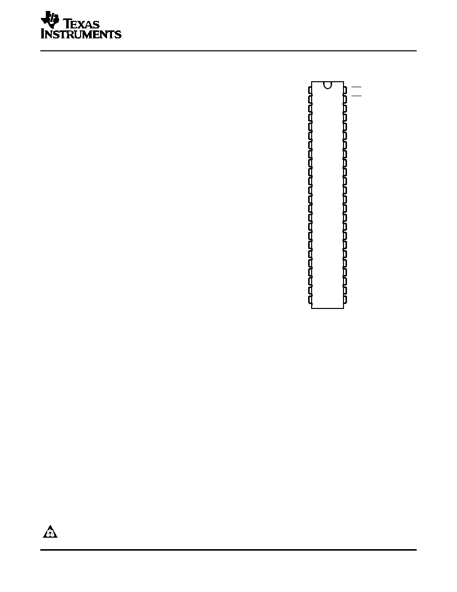
DGG OR DGV PACKAGE
(TOP VIEW)
NC - No internal connection
1
2
3
4
5
6
7
8
9
10
11
12
13
14
15
16
17
18
19
20
21
22
23
24
48
47
46
45
44
43
42
41
40
39
38
37
36
35
34
33
32
31
30
29
28
27
26
25
NC
1A1
1A2
1A3
1A4
1A5
1A6
GND
1A7
1A8
1A9
1A10
2A1
2A2
VCC
2A3
GND
2A4
2A5
2A6
2A7
2A8
2A9
2A10
1OE
2OE
1B1
1B2
1B3
1B4
1B5
GND
1B6
1B7
1B8
1B9
1B10
2B1
2B2
2B3
GND
2B4
2B5
2B6
2B7
2B8
2B9
2B10
DESCRIPTION/ORDERING INFORMATION
SN74CB3T16210
20-BIT FET BUS SWITCH
2.5-V/3.3-V LOW-VOLTAGE BUS SWITCH WITH 5-V-TOLERANT LEVEL SHIFTER
SCDS156A – OCTOBER 2003 – REVISED MARCH 2005
Member of the Texas Instruments Widebus
Family
Output Voltage Translation Tracks VCC
Supports Mixed-Mode Signal Operation on All
Data I/O Ports
– 5-V Input Down to 3.3-V Output Level Shift
With 3.3-V VCC
– 5-V/3.3-V Input Down to 2.5-V Output Level
Shift With 2.5-V VCC
5-V-Tolerant I/Os With Device Powered Up or
Powered Down
Bidirectional Data Flow With Near-Zero
Propagation Delay
Low ON-State Resistance (ron) Characteristics
(ron = 5 Typ)
Low Input/Output Capacitance Minimizes
Loading (Cio(OFF) = 5 pF Typ)
Data and Control Inputs Provide Undershoot
Clamp Diodes
Low Power Consumption
(ICC = 40 A Max)
VCC Operating Range From 2.3 V to 3.6 V
Data I/Os Support 0- to 5-V Signaling Levels
(0.8 V, 1.2 V, 1.5 V, 1.8 V, 2.5 V, 3.3 V, 5 V)
Control Inputs Can Be Driven by TTL or
5-V/3.3-V CMOS Outputs
Ioff Supports Partial-Power-Down Mode
Operation
Latch-Up Performance Exceeds 250 mA Per
JESD 17
ESD Performance Tested Per JESD 22
– 2000-V Human-Body Model
(A114-B, Class II)
– 1000-V Charged-Device Model (C101)
Supports Digital Applications: Level
Translation, PCI Interface, USB Interface,
Memory Interleaving, and Bus Isolation
Ideal for Low-Power Portable Equipment
The SN74CB3T16210 is a high-speed TTL-compatible FET bus switch with low ON-state resistance (ron),
allowing for minimal propagation delay. The device fully supports mixed-mode signal operation on all data I/O
ports by providing voltage translation that tracks VCC. The SN74CB3T16210 supports systems using 5-V TTL,
3.3-V LVTTL, and 2.5-V CMOS switching standards, as well as user-defined switching levels (see Figure 1).
Please be aware that an important notice concerning availability, standard warranty, and use in critical applications of Texas
Instruments semiconductor products and disclaimers thereto appears at the end of this data sheet.
Widebus is a trademark of Texas Instruments.
PRODUCTION DATA information is current as of publication date.
Copyright 2003–2005, Texas Instruments Incorporated
Products conform to specifications per the terms of the Texas
Instruments standard warranty. Production processing does not
necessarily include testing of all parameters.
相关PDF资料 |
PDF描述 |
|---|---|
| SN74CB3T16212DGGR | CB3T/3VT SERIES, 12 2-BIT EXCHANGER, TRUE OUTPUT, PDSO56 |
| SN74CB3T3245DWRE4 | CB3T/3VT SERIES, 8-BIT DRIVER, TRUE OUTPUT, PDSO20 |
| SN74CB3T3245DWG4 | CB3T/3VT SERIES, 8-BIT DRIVER, TRUE OUTPUT, PDSO20 |
| SN74CB3T3257PW | CB3T/3VT SERIES, QUAD 1 LINE TO 2 LINE MULTIPLEXER AND DEMUX/DECODER, TRUE OUTPUT, PDSO16 |
| SN74CB3T3306DCTR | CB3T/3VT SERIES, DUAL 1-BIT DRIVER, TRUE OUTPUT, PDSO8 |
相关代理商/技术参数 |
参数描述 |
|---|---|
| SN74CB3T16210DGGR | 功能描述:数字总线开关 IC 20B FET Bus Switch RoHS:否 制造商:Texas Instruments 开关数量:24 传播延迟时间:0.25 ns 最大工作温度:+ 85 C 最小工作温度:- 40 C 封装 / 箱体:TSSOP-56 封装:Reel |
| SN74CB3T16210DGGR | 制造商:Texas Instruments 功能描述:IC SWITCH BUS 20BIT FET 48TSSOP 制造商:Texas Instruments 功能描述:IC, SWITCH, BUS, 20BIT, FET, 48TSSOP |
| SN74CB3T16210DGGR | 制造商:Texas Instruments 功能描述:Switch Logic IC |
| SN74CB3T16210DGVR | 功能描述:数字总线开关 IC 20B FET Bus Switch RoHS:否 制造商:Texas Instruments 开关数量:24 传播延迟时间:0.25 ns 最大工作温度:+ 85 C 最小工作温度:- 40 C 封装 / 箱体:TSSOP-56 封装:Reel |
| SN74CB3T16211DGG | 制造商:Rochester Electronics LLC 功能描述:- Bulk 制造商:Texas Instruments 功能描述: |
发布紧急采购,3分钟左右您将得到回复。