参数资料
| 型号: | SN74CB3T3245DWE4 |
| 厂商: | Texas Instruments |
| 文件页数: | 16/21页 |
| 文件大小: | 0K |
| 描述: | IC SWITCH BUS FET HS 20-SOIC |
| 标准包装: | 25 |
| 系列: | 74CB |
| 类型: | FET 总线开关 |
| 电路: | 8 x 1:1 |
| 独立电路: | 1 |
| 输出电流高,低: | 32mA,64mA |
| 电压电源: | 单电源 |
| 电源电压: | 2.3 V ~ 3.6 V |
| 工作温度: | -40°C ~ 85°C |
| 安装类型: | 表面贴装 |
| 封装/外壳: | 20-SOIC(0.295",7.50mm 宽) |
| 供应商设备封装: | 20-SOIC |
| 包装: | 管件 |
SCDS136A – OCTOBER 2003 – REVISED AUGUST 2012
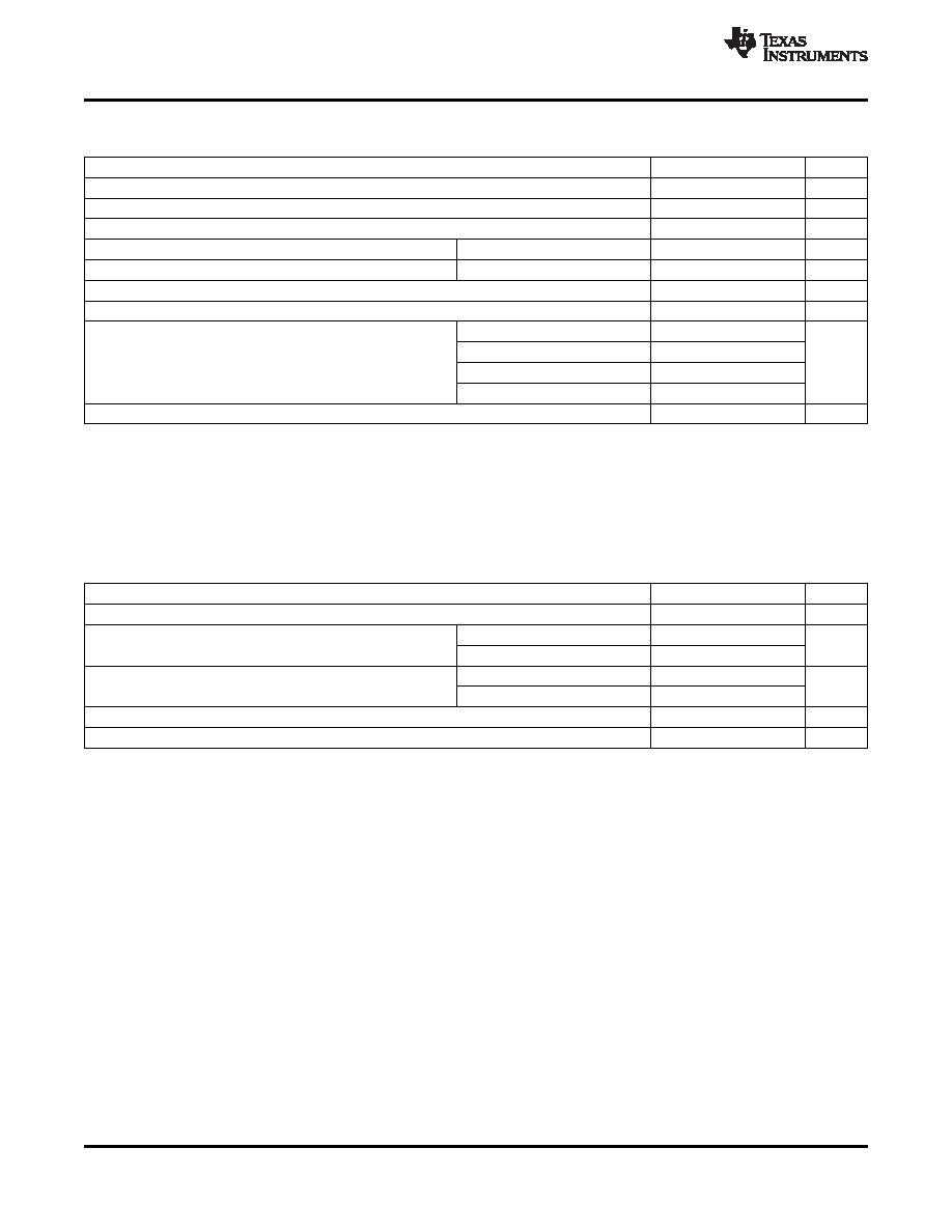
Absolute Maximum Ratings
(1)
over operating free-air temperature range (unless otherwise noted)
MIN
MAX
UNIT
VCC
Supply voltage range(2)
–0.5
7
V
VIN
Control input voltage range(2) (3)
–0.5
7
V
VI/O
Switch I/O voltage range(2) (3) (4)
–0.5
7
V
IIK
Control input clamp current
VIN < 0
–50
mA
II/OK
I/O port clamp current
VI/O < 0
–50
mA
II/O
ON-state switch current(5)
±128
mA
Continuous current through VCC or GND
±100
mA
DBQ package
68
DGV package
92
θJA
Package thermal impedance(6)
°C/W
DW package
58
PW package
83
Tstg
Storage temperature range
–65
150
°C
(1)
Stresses beyond those listed under "absolute maximum ratings" may cause permanent damage to the device. These are stress ratings
only, and functional operation of the device at these or any other conditions beyond those indicated under "recommended operating
conditions" is not implied. Exposure to absolute-maximum-rated conditions for extended periods may affect device reliability.
(2)
All voltages are with respect to ground unless otherwise specified.
(3)
The input and output voltage ratings may be exceeded if the input and output clamp-current ratings are observed.
(4)
VI and VO are used to denote specific conditions for VI/O.
(5)
II and IO are used to denote specific conditions for II/O.
(6)
The package thermal impedance is calculated in accordance with JESD 51-7.
Recommended Operating Conditions
(1)
MIN
MAX
UNIT
VCC
Supply voltage
2.3
3.6
V
VCC = 2.3 V to 2.7 V
1.7
5.5
VIH
High-level control input voltage
V
VCC = 2.7 V to 3.6 V
2
5.5
VCC = 2.3 V to 2.7 V
0
0.7
VIL
Low-level control input voltage
V
VCC = 2.7 V to 3.6 V
0
0.8
VI/O
Data input/output voltage
0
5.5
V
TA
Operating free-air temperature
–40
85
°C
(1)
All unused control inputs of the device must be held at VCC or GND to ensure proper device operation. Refer to the TI application report,
Implications of Slow or Floating CMOS Inputs, literature number SCBA004.
4
Copyright 2003–2012, Texas Instruments Incorporated
Product Folder Links: SN74CB3T3245
相关PDF资料 |
PDF描述 |
|---|---|
| VI-B61-MY-F4 | CONVERTER MOD DC/DC 12V 50W |
| SN74CB3T3245DW | IC SWITCH BUS FET HS 20-SOIC |
| VE-J5M-MZ-S | CONVERTER MOD DC/DC 10V 25W |
| VI-B61-MY-F3 | CONVERTER MOD DC/DC 12V 50W |
| DS1020S-15+T | IC DELAY LINE 256TAP 16-SOIC |
相关代理商/技术参数 |
参数描述 |
|---|---|
| SN74CB3T3245DWG4 | 功能描述:数字总线开关 IC 8B FET 2.5V 3.3V LO VLTG Bus Switch RoHS:否 制造商:Texas Instruments 开关数量:24 传播延迟时间:0.25 ns 最大工作温度:+ 85 C 最小工作温度:- 40 C 封装 / 箱体:TSSOP-56 封装:Reel |
| SN74CB3T3245DWR | 功能描述:数字总线开关 IC 8-Bit FET 2.5/3.3V Lo-Vltg Bus Switch RoHS:否 制造商:Texas Instruments 开关数量:24 传播延迟时间:0.25 ns 最大工作温度:+ 85 C 最小工作温度:- 40 C 封装 / 箱体:TSSOP-56 封装:Reel |
| SN74CB3T3245DWRE4 | 功能描述:数字总线开关 IC 3.3-V ABT Octal Bus Trncvr W/3-St Otpt RoHS:否 制造商:Texas Instruments 开关数量:24 传播延迟时间:0.25 ns 最大工作温度:+ 85 C 最小工作温度:- 40 C 封装 / 箱体:TSSOP-56 封装:Reel |
| SN74CB3T3245DWRG4 | 功能描述:数字总线开关 IC 8B FET 2.5V 3.3V LO VLTG Bus Switch RoHS:否 制造商:Texas Instruments 开关数量:24 传播延迟时间:0.25 ns 最大工作温度:+ 85 C 最小工作温度:- 40 C 封装 / 箱体:TSSOP-56 封装:Reel |
| SN74CB3T3245PW | 功能描述:数字总线开关 IC 8-Bit FET 2.5/3.3V Lo-Vltg Bus Switch RoHS:否 制造商:Texas Instruments 开关数量:24 传播延迟时间:0.25 ns 最大工作温度:+ 85 C 最小工作温度:- 40 C 封装 / 箱体:TSSOP-56 封装:Reel |
发布紧急采购,3分钟左右您将得到回复。