- 您现在的位置:买卖IC网 > PDF目录98110 > SN74CBTD3305CPWRG3 (TEXAS INSTRUMENTS INC) CBT/FST/QS/5C/B SERIES, DUAL 1-BIT DRIVER, TRUE OUTPUT, PDSO8 PDF资料下载
参数资料
| 型号: | SN74CBTD3305CPWRG3 |
| 厂商: | TEXAS INSTRUMENTS INC |
| 元件分类: | 总线收发器 |
| 英文描述: | CBT/FST/QS/5C/B SERIES, DUAL 1-BIT DRIVER, TRUE OUTPUT, PDSO8 |
| 封装: | PLASTIC, TSSOP-8 |
| 文件页数: | 11/16页 |
| 文件大小: | 436K |
| 代理商: | SN74CBTD3305CPWRG3 |
SN74CBTD3305C
DUAL FET BUS SWITCH WITH LEVEL SHIFTING
5-V BUS SWITCH WITH –2-V UNDERSHOOT PROTECTION
SCDS126A SEPTEMBER 2003 REVISED OCTOBER 2003
4
POST OFFICE BOX 655303
DALLAS, TEXAS 75265
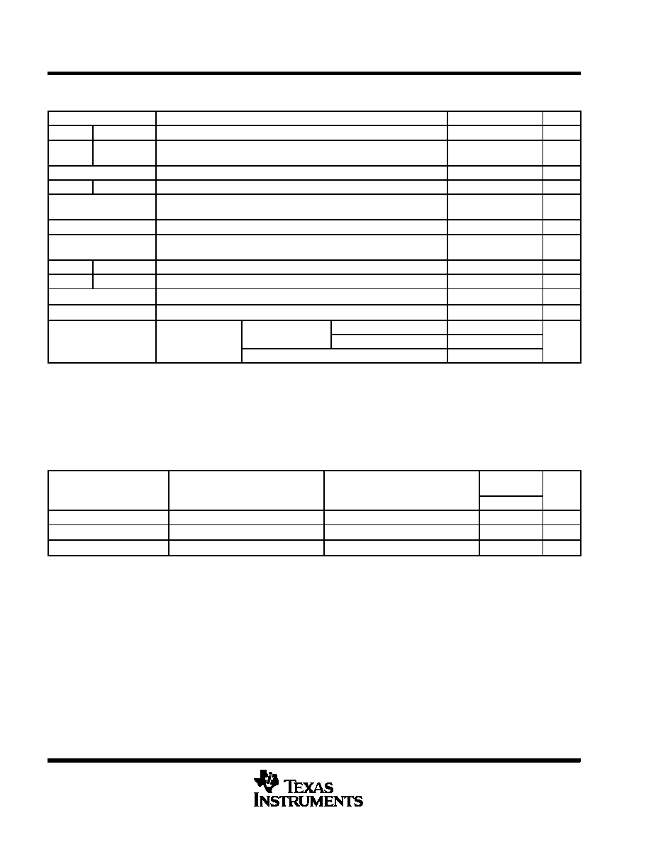
electrical characteristics over recommended operating free-air temperature range (unless
otherwise noted)
PARAMETER
TEST CONDITIONS
MIN
TYP
MAX
UNIT
VIK
Control inputs
VCC = 4.5 V,
IIN = 18 mA
1.8
V
VIKU
Data inputs
VCC = 5 V,
0 mA
> II ≥ 50 mA,
VIN = VCC or GND,
Switch OFF
2
V
VOH
See Figures 4 and 5
IIN
Control inputs
VCC = 5.5 V,
VIN = VCC or GND
±1
μA
IOZ
VCC = 5.5 V,
VO = 0 to 5.5 V,
VI = 0,
Switch OFF,
VIN = VCC or GND
±10
μA
Ioff
VCC = 0,
VO = 0 to 5.5 V,
VI = 0
10
μA
ICC
VCC = 5.5 V,
II/O = 0,
VIN = VCC or GND,
Switch ON or OFF
1.5
mA
ΔICC§
Control inputs
VCC = 5.5 V,
One input at 3.4 V,
Other inputs at VCC or GND
2.5
mA
Cin
Control inputs
VIN = 3 V or 0
3.5
pF
Cio(OFF)
VI/O = 3 V or 0,
Switch OFF,
VIN = VCC or GND
5
pF
Cio(ON)
VI/O = 3 V or 0,
Switch ON,
VIN = VCC or GND
12.5
pF
V
0
IO = 64 mA
3
6
ron
VCC = 4.5 V
VI = 0
IO = 30 mA
3
6
Ω
on
CC
VI = 2.4 V,
IO = 15 mA
8
20
VIN and IIN refer to control inputs. VI, VO, II, and IO refer to data pins.
All typical values are at VCC = 5 V (unless otherwise noted), TA = 25°C.
For I/O ports, the parameter IOZ includes the input leakage current.
§ This is the increase in supply current for each input that is at the specified voltage level, rather than VCC or GND.
Measured by the voltage drop between the A and B terminals at the indicated current through the switch. ON-state resistance is determined by
the lower of the voltages of the two (A or B) terminals.
switching characteristics over recommended operating free-air temperature range (unless
otherwise noted) (see Figure 3)
PARAMETER
FROM
(INPUT)
TO
(OUTPUT)
VCC = 5 V
± 0.5 V
UNIT
PARAMETER
(INPUT)
(OUTPUT)
MIN
MAX
UNIT
tpd#
A or B
B or A
0.15
ns
ten
OE
A or B
1.5
4.7
ns
tdis
OE
A or B
1.5
5.3
ns
# The propagation delay is the calculated RC time constant of the typical ON-state resistance of the switch and the specified load capacitance,
when driven by an ideal voltage source (zero output impedance).
相关PDF资料 |
PDF描述 |
|---|---|
| SN74CBTD3306CPW | CBT/FST/QS/5C/B SERIES, DUAL 1-BIT DRIVER, TRUE OUTPUT, PDSO8 |
| SN74CBTD3306DR | CBT/FST/QS/5C/B SERIES, DUAL 1-BIT DRIVER, TRUE OUTPUT, PDSO8 |
| SN74CBTD3306PWRG3 | CBT/FST/QS/5C/B SERIES, DUAL 1-BIT DRIVER, TRUE OUTPUT, PDSO8 |
| SN74CBTD3384CDB | CBT/FST/QS/5C/B SERIES, 10 1-BIT DRIVER, TRUE OUTPUT, PDSO24 |
| SN74CBTD3384PWG4 | CBT/FST/QS/5C/B SERIES, DUAL 5-BIT DRIVER, TRUE OUTPUT, PDSO24 |
相关代理商/技术参数 |
参数描述 |
|---|---|
| SN74CBTD3305CPWRG4 | 功能描述:数字总线开关 IC Dual FETBus Switch RoHS:否 制造商:Texas Instruments 开关数量:24 传播延迟时间:0.25 ns 最大工作温度:+ 85 C 最小工作温度:- 40 C 封装 / 箱体:TSSOP-56 封装:Reel |
| SN74CBTD3306CD | 功能描述:数字总线开关 IC Dual FET Bus Switch RoHS:否 制造商:Texas Instruments 开关数量:24 传播延迟时间:0.25 ns 最大工作温度:+ 85 C 最小工作温度:- 40 C 封装 / 箱体:TSSOP-56 封装:Reel |
| SN74CBTD3306CD | 制造商:Texas Instruments 功能描述:Switch Logic IC |
| SN74CBTD3306CDE4 | 功能描述:数字总线开关 IC Dual FET Bus Switch RoHS:否 制造商:Texas Instruments 开关数量:24 传播延迟时间:0.25 ns 最大工作温度:+ 85 C 最小工作温度:- 40 C 封装 / 箱体:TSSOP-56 封装:Reel |
| SN74CBTD3306CDG4 | 功能描述:数字总线开关 IC Dual FETBus Switch RoHS:否 制造商:Texas Instruments 开关数量:24 传播延迟时间:0.25 ns 最大工作温度:+ 85 C 最小工作温度:- 40 C 封装 / 箱体:TSSOP-56 封装:Reel |
发布紧急采购,3分钟左右您将得到回复。