- 您现在的位置:买卖IC网 > PDF目录98111 > SN74CBTK6800DWE4 (TEXAS INSTRUMENTS INC) CBT/FST/QS/5C/B SERIES, 10-BIT DRIVER, TRUE OUTPUT, PDSO24 PDF资料下载
参数资料
| 型号: | SN74CBTK6800DWE4 |
| 厂商: | TEXAS INSTRUMENTS INC |
| 元件分类: | 总线收发器 |
| 英文描述: | CBT/FST/QS/5C/B SERIES, 10-BIT DRIVER, TRUE OUTPUT, PDSO24 |
| 封装: | PLASTIC, SOIC-24 |
| 文件页数: | 1/15页 |
| 文件大小: | 496K |
| 代理商: | SN74CBTK6800DWE4 |
SN74CBTK6800
10-BIT FET BUS SWITCH WITH PRECHARGED OUTPUTS
AND ACTIVE-CLAMP UNDERSHOOT-PROTECTION CIRCUIT
SCDS107B – APRIL 2000 – REVISED OCTOBER 2000
1
POST OFFICE BOX 655303
DALLAS, TEXAS 75265
D 5- Switch Connection Between Two Ports
D TTL-Compatible Input Levels
D Power Off Disables Outputs, Permitting
Live Insertion
D Outputs Are Precharged by Bias Voltage to
Minimize Signal Distortion During Live
Insertion
D Active-Clamp Undershoot-Protection
Circuit on the I/Os Clamps Undershoots
Down to –2 V
D Latch-Up Performance Exceeds 100 mA Per
JESD 78, Class II
D ESD Protection Exceeds JESD 22
– 2000-V Human-Body Model (A114-A)
– 200-V Machine Model (A115-A)
– 1000-V Charged-Device Model (C101)
description
The SN74CBTK6800 device provides ten bits of high-speed TTL-compatible bus switching. The low on-state
resistance of the switch allows bidirectional connections to be made while adding near-zero propagation delay.
The device also precharges the B port to a user-selectable bias voltage (BIASV) to minimize live-insertion noise.
The A and B ports have an active-clamp undershoot-protection circuit. When there is an undershoot, the
active-clamp circuit is enabled and current from VCC is supplied to clamp the output, preventing the pass
transistor from turning on.
The SN74CBTK6800 is organized as one 10-bit switch with a single enable (ON) input. When ON is low, the
switch is on, and port A is connected to port B. When ON is high, the switch between port A and port B is open.
When ON is high or VCC is 0 V, B port is precharged to BIASV through the equivalent of a 10-k resistor.
ORDERING INFORMATION
TA
PACKAGE
ORDERABLE
PART NUMBER
TOP-SIDE
MARKING
SOIC
DW
Tube
SN74CBTK6800DW
CBTK6800
SOIC – DW
Tape and reel
SN74CBTK6800DWR
CBTK6800
–40
°C to 85°C
SSOP (QSOP) – DBQ
Tape and reel
SN74CBTK6800DBQR
CBTK6800
TSSOP – PW
Tape and reel
SN74CBTK6800PWR
BK6800
TVSOP – DGV
Tape and reel
SN74CBTK6800DGVR
BK6800
Package drawings, standard packing quantities, thermal data, symbolization, and PCB design guidelines
are available at www.ti.com/sc/package.
FUNCTION TABLE
INPUT
ON
FUNCTION
L
A port = B port
H
A port = Z
B port = BIASV
Please be aware that an important notice concerning availability, standard warranty, and use in critical applications of
Texas Instruments semiconductor products and disclaimers thereto appears at the end of this data sheet.
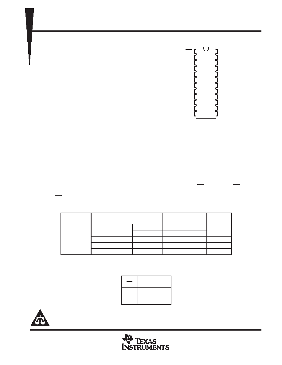
DBQ, DGV, DW, OR PW PACKAGE
(TOP VIEW)
ON
A1
A2
A3
A4
A5
A6
A7
A8
A9
A10
GND
VCC
B1
B2
B3
B4
B5
B6
B7
B8
B9
B10
BIASV
1
2
3
4
5
6
7
8
9
10
11
12
24
23
22
21
20
19
18
17
16
15
14
13
Copyright
2000, Texas Instruments Incorporated
PRODUCTION DATA information is current as of publication date.
Products conform to specifications per the terms of Texas Instruments
standard warranty. Production processing does not necessarily include
testing of all parameters.
相关PDF资料 |
PDF描述 |
|---|---|
| SN74CBTK6800DWRG4 | CBT/FST/QS/5C/B SERIES, 10-BIT DRIVER, TRUE OUTPUT, PDSO24 |
| SN74CBTLV16212DL | CBTLV/3B SERIES, 24-BIT EXCHANGER, TRUE OUTPUT, PDSO56 |
| SN74CBTLV3125NSR | CBTLV/3B SERIES, 4-BIT DRIVER, TRUE OUTPUT, PDSO14 |
| SN74CBTLV3125PW | CBTLV/3B SERIES, QUAD 1-BIT DRIVER, TRUE OUTPUT, PDSO14 |
| SN74CBTLV3126DBQR | CBTLV/3B SERIES, 4-BIT DRIVER, TRUE OUTPUT, PDSO16 |
相关代理商/技术参数 |
参数描述 |
|---|---|
| SN74CBTK6800DWG4 | 功能描述:数字总线开关 IC 10B FETBus Switch RoHS:否 制造商:Texas Instruments 开关数量:24 传播延迟时间:0.25 ns 最大工作温度:+ 85 C 最小工作温度:- 40 C 封装 / 箱体:TSSOP-56 封装:Reel |
| SN74CBTK6800DWR | 功能描述:数字总线开关 IC 10bit FET RoHS:否 制造商:Texas Instruments 开关数量:24 传播延迟时间:0.25 ns 最大工作温度:+ 85 C 最小工作温度:- 40 C 封装 / 箱体:TSSOP-56 封装:Reel |
| SN74CBTK6800DWRE4 | 功能描述:数字总线开关 IC Octal Buffer/Driver With 3-State Outputs RoHS:否 制造商:Texas Instruments 开关数量:24 传播延迟时间:0.25 ns 最大工作温度:+ 85 C 最小工作温度:- 40 C 封装 / 箱体:TSSOP-56 封装:Reel |
| SN74CBTK6800DWRG4 | 功能描述:数字总线开关 IC 10B FETBus Switch RoHS:否 制造商:Texas Instruments 开关数量:24 传播延迟时间:0.25 ns 最大工作温度:+ 85 C 最小工作温度:- 40 C 封装 / 箱体:TSSOP-56 封装:Reel |
| SN74CBTK6800GVR | 制造商:Rochester Electronics LLC 功能描述:- Bulk 制造商:Texas Instruments 功能描述: |
发布紧急采购,3分钟左右您将得到回复。