- 您现在的位置:买卖IC网 > PDF目录373477 > SN74HC7032NSRE4 (Texas Instruments, Inc.) QUADRUPLE POSITIVE-OR GATES WITH SCHMITT-TRIGGER INPUTS PDF资料下载
参数资料
| 型号: | SN74HC7032NSRE4 |
| 厂商: | Texas Instruments, Inc. |
| 英文描述: | QUADRUPLE POSITIVE-OR GATES WITH SCHMITT-TRIGGER INPUTS |
| 中文描述: | 翻两番积极方式或与施密特盖茨触发输入 |
| 文件页数: | 2/9页 |
| 文件大小: | 321K |
| 代理商: | SN74HC7032NSRE4 |
SCLS036E MARCH 1984 REVISED NOVEMBER 2004
2
POST OFFICE BOX 655303
DALLAS, TEXAS 75265
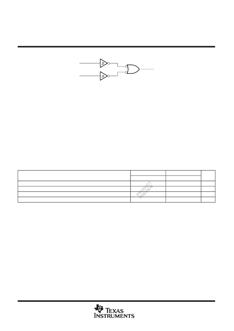
logic diagram, each gate (positive logic)
A
B
Y
absolute maximum ratings over operating free-air temperature range (unless otherwise noted)
Supply voltage range, V
CC
Input clamp current, I
IK
(V
I
< 0 or V
I
> V
CC
) (see Note 1)
Output clamp current, I
OK
(V
O
< 0 or V
O
> V
CC
) (see Note 1)
Continuous output current, I
O
(V
O
= 0 to V
CC
)
Continuous current through V
CC
or GND
Package thermal impedance,
θ
JA
(see Note 2): D package
0.5 V to 7 V
±
20 mA
±
20 mA
±
25 mA
±
50 mA
86
°
C/W
80
°
C/W
76
°
C/W
65
°
C to 150
°
C
. . . . . . . . . . . . . . . . . . . . . . . . . . . . . . . . . . . . . . . . . . . . . . . . . . . . . . . . . .
. . . . . . . . . . . . . . . . . . . . . . . . . . . . . . . . . . . .
. . . . . . . . . . . . . . . . . . . . . . . . . . . . . . . .
. . . . . . . . . . . . . . . . . . . . . . . . . . . . . . . . . . . . . . . . . . . . . .
. . . . . . . . . . . . . . . . . . . . . . . . . . . . . . . . . . . . . . . . . . . . . . . . . . .
. . . . . . . . . . . . . . . . . . . . . . . . . . . . . . . . . . .
N package
. . . . . . . . . . . . . . . . . . . . . . . . . . . . . . . . . . .
NS package
. . . . . . . . . . . . . . . . . . . . . . . . . . . . . . . . .
Storage temperature range, T
stg
. . . . . . . . . . . . . . . . . . . . . . . . . . . . . . . . . . . . . . . . . . . . . . . . . . .
Stresses beyond those listed under “absolute maximum ratings” may cause permanent damage to the device. These are stress ratings only, and
functional operation of the device at these or any other conditions beyond those indicated under “recommended operating conditions” is not
implied. Exposure to absolute-maximum-rated conditions for extended periods may affect device reliability.
NOTES:
1. The input and output voltage ratings may be exceeded if the input and output current ratings are observed.
2. The package thermal impedance is calculated in accordance with JESD 51-7.
recommended operating conditions (see Note 3)
SN54HC7032
MIN
NOM
SN74HC7032
MIN
NOM
UNIT
MAX
MAX
VCC
VI
VO
TA
NOTE 3: All unused inputs of the device must be held at VCC or GND to ensure proper device operation. Refer to the TI application report,
Implications of Slow or Floating CMOS Inputs
, literature number SCBA004.
Supply voltage
2
5
6
2
5
6
V
Input voltage
0
VCC
VCC
125
0
VCC
VCC
85
V
Output voltage
0
0
V
°
C
Operating free-air temperature
55
40
')"*%("' #"'#&*' +*"!$# ' & )"*%(3& "*
") !&3&-"+%&'. (*(#&*#
(*& !&2' 2"(-. &/(
'*$%&'
#('2& "* !#"''$&
&&
+*"!$# 0"$
!&2' +(&
+&#)#("'
!(( ('! "&*
*&&*3&
'"#&.
& *2
"
相关PDF资料 |
PDF描述 |
|---|---|
| SN74HC7032DRE4 | QUADRUPLE POSITIVE-OR GATES WITH SCHMITT-TRIGGER INPUTS |
| SN74HC7032NSR | QUADRUPLE POSITIVE-OR GATES WITH SCHMITT-TRIGGER INPUTS |
| SN74HCT245DB | 1A, 18V,±4% Tolerance, Voltage Regulator, Ta = 0°C to +125°C; Package: 3 LEAD D2PAK; No of Pins: 3; Container: Tape and Reel; Qty per Container: 800 |
| SN54HCT245FK | 4.27V Voltage Detector with Active Low Open Collector Output for 5V Systems; Package: Micro8™; No of Pins: 8; Container: Tape and Reel; Qty per Container: 4000 |
| SN54HCT245W | OCTAL BUS TRANSCEIVERS WITH 3-STATE OUTPUTS |
相关代理商/技术参数 |
参数描述 |
|---|---|
| SN74HC7032NSRG4 | 功能描述:逻辑门 Quad Pos OR Gates RoHS:否 制造商:Texas Instruments 产品:OR 逻辑系列:LVC 栅极数量:2 线路数量(输入/输出):2 / 1 高电平输出电流:- 16 mA 低电平输出电流:16 mA 传播延迟时间:3.8 ns 电源电压-最大:5.5 V 电源电压-最小:1.65 V 最大工作温度:+ 125 C 安装风格:SMD/SMT 封装 / 箱体:DCU-8 封装:Reel |
| SN74HC7266N | 制造商:Rochester Electronics LLC 功能描述:- Bulk 制造商:Texas Instruments 功能描述: |
| SN74HC74ADBR | 制造商:Rochester Electronics LLC 功能描述:- Bulk |
| SN74HC74AN | 制造商:Texas Instruments 功能描述: |
| SN74HC74AN-P2 | 制造商:Texas Instruments 功能描述: |
发布紧急采购,3分钟左右您将得到回复。