- 您现在的位置:买卖IC网 > PDF目录98120 > SN74LV373ADWE4 (TEXAS INSTRUMENTS INC) LV/LV-A/LVX/H SERIES, 8-BIT DRIVER, TRUE OUTPUT, PDSO20 PDF资料下载
参数资料
| 型号: | SN74LV373ADWE4 |
| 厂商: | TEXAS INSTRUMENTS INC |
| 元件分类: | 总线收发器 |
| 英文描述: | LV/LV-A/LVX/H SERIES, 8-BIT DRIVER, TRUE OUTPUT, PDSO20 |
| 封装: | GREEN, PLASTIC, SOIC-20 |
| 文件页数: | 12/23页 |
| 文件大小: | 913K |
| 代理商: | SN74LV373ADWE4 |
SN54LV373A, SN74LV373A
OCTAL TRANSPARENT DTYPE LATCHES
WITH 3STATE OUTPUTS
SCLS407J APRIL 1998 REVISED APRIL 2005
2
POST OFFICE BOX 655303
DALLAS, TEXAS 75265
description/ordering information (continued)
While the latch-enable (LE) input is high, the Q outputs follow the data (D) inputs. When LE is taken low, the
Q outputs are latched at the logic levels set up at the D inputs.
A buffered output-enable (OE) input can be used to place the eight outputs in either a normal logic state (high
or low) or the high-impedance state. In the high-impedance state, the outputs neither load nor drive the bus lines
significantly. The high-impedance state and increased drive provide the capability to drive bus lines without
need for interface or pullup components.
OE does not affect the internal operations of the latches. Old data can be retained or new data can be entered
while the outputs are in the high-impedance state.
To ensure the high-impedance state during power up or power down, OE should be tied to VCC through a pullup
resistor; the minimum value of the resistor is determined by the current-sinking capability of the driver.
These devices are fully specified for partial-power-down applications using Ioff. The Ioff circuitry disables the
outputs, preventing damaging current backflow through the devices when they are powered down.
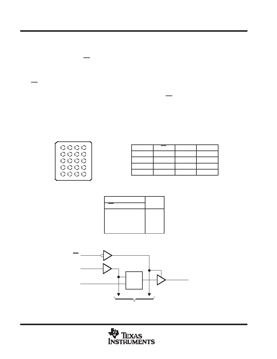
terminal assignments
1234
A
1Q
OE
VCC
8Q
B
2D
7D
1D
8D
C
3Q
2Q
6Q
7Q
D
4D
5D
3D
6D
E
GND
4Q
LE
5Q
FUNCTION TABLE
(each latch)
INPUTS
OUTPUT
OE
LE
D
OUTPUT
Q
L
H
L
HL
L
LX
Q0
H
X
Z
logic diagram (positive logic)
OE
To Seven Other Channels
1
11
3
2
LE
1D
C1
1D
1Q
Pin numbers shown are for the DB, DGV, DW, FK, J, NS, PW, RGY, and W packages.
GQN PACKAGE
(TOP VIEW)
1
234
A
B
C
D
E
相关PDF资料 |
PDF描述 |
|---|---|
| SN74LV373APWRE4 | LV/LV-A/LVX/H SERIES, 8-BIT DRIVER, TRUE OUTPUT, PDSO20 |
| SN74LV373ATNSR | LV/LV-A/LVX/H SERIES, 8-BIT DRIVER, TRUE OUTPUT, PDSO20 |
| SN74LV373ATPW | LV/LV-A/LVX/H SERIES, 8-BIT DRIVER, TRUE OUTPUT, PDSO20 |
| SN74LV374ADGVRG4 | LV/LV-A/LVX/H SERIES, 8-BIT DRIVER, TRUE OUTPUT, PDSO20 |
| SN74LV374ADGVRE4 | LV/LV-A/LVX/H SERIES, 8-BIT DRIVER, TRUE OUTPUT, PDSO20 |
相关代理商/技术参数 |
参数描述 |
|---|---|
| SN74LV373ADWG4 | 功能描述:闭锁 Octal Transp DType Latch RoHS:否 制造商:Micrel 电路数量:1 逻辑类型:CMOS 逻辑系列:TTL 极性:Non-Inverting 输出线路数量:9 高电平输出电流: 低电平输出电流: 传播延迟时间: 电源电压-最大:12 V 电源电压-最小:5 V 最大工作温度:+ 85 C 最小工作温度:- 40 C 封装 / 箱体:SOIC-16 封装:Reel |
| SN74LV373ADWR | 功能描述:闭锁 Octal Trans D-Type 闭锁 RoHS:否 制造商:Micrel 电路数量:1 逻辑类型:CMOS 逻辑系列:TTL 极性:Non-Inverting 输出线路数量:9 高电平输出电流: 低电平输出电流: 传播延迟时间: 电源电压-最大:12 V 电源电压-最小:5 V 最大工作温度:+ 85 C 最小工作温度:- 40 C 封装 / 箱体:SOIC-16 封装:Reel |
| SN74LV373ADWRE4 | 功能描述:闭锁 Octal Transp DType Latch RoHS:否 制造商:Micrel 电路数量:1 逻辑类型:CMOS 逻辑系列:TTL 极性:Non-Inverting 输出线路数量:9 高电平输出电流: 低电平输出电流: 传播延迟时间: 电源电压-最大:12 V 电源电压-最小:5 V 最大工作温度:+ 85 C 最小工作温度:- 40 C 封装 / 箱体:SOIC-16 封装:Reel |
| SN74LV373ADWRG4 | 功能描述:闭锁 Octal Transp DType Latch RoHS:否 制造商:Micrel 电路数量:1 逻辑类型:CMOS 逻辑系列:TTL 极性:Non-Inverting 输出线路数量:9 高电平输出电流: 低电平输出电流: 传播延迟时间: 电源电压-最大:12 V 电源电压-最小:5 V 最大工作温度:+ 85 C 最小工作温度:- 40 C 封装 / 箱体:SOIC-16 封装:Reel |
| SN74LV373AGQNR | 功能描述:闭锁 Tri-St Octal D-Type RoHS:否 制造商:Micrel 电路数量:1 逻辑类型:CMOS 逻辑系列:TTL 极性:Non-Inverting 输出线路数量:9 高电平输出电流: 低电平输出电流: 传播延迟时间: 电源电压-最大:12 V 电源电压-最小:5 V 最大工作温度:+ 85 C 最小工作温度:- 40 C 封装 / 箱体:SOIC-16 封装:Reel |
发布紧急采购,3分钟左右您将得到回复。