- 您现在的位置:买卖IC网 > PDF目录98123 > SN74LVC1G14YZTR (TEXAS INSTRUMENTS INC) LVC/LCX/Z SERIES, 1-INPUT INVERT GATE, BGA4 PDF资料下载
参数资料
| 型号: | SN74LVC1G14YZTR |
| 厂商: | TEXAS INSTRUMENTS INC |
| 元件分类: | 门电路 |
| 英文描述: | LVC/LCX/Z SERIES, 1-INPUT INVERT GATE, BGA4 |
| 封装: | GREEN, DSBGA-5 |
| 文件页数: | 13/19页 |
| 文件大小: | 741K |
| 代理商: | SN74LVC1G14YZTR |
www.ti.com
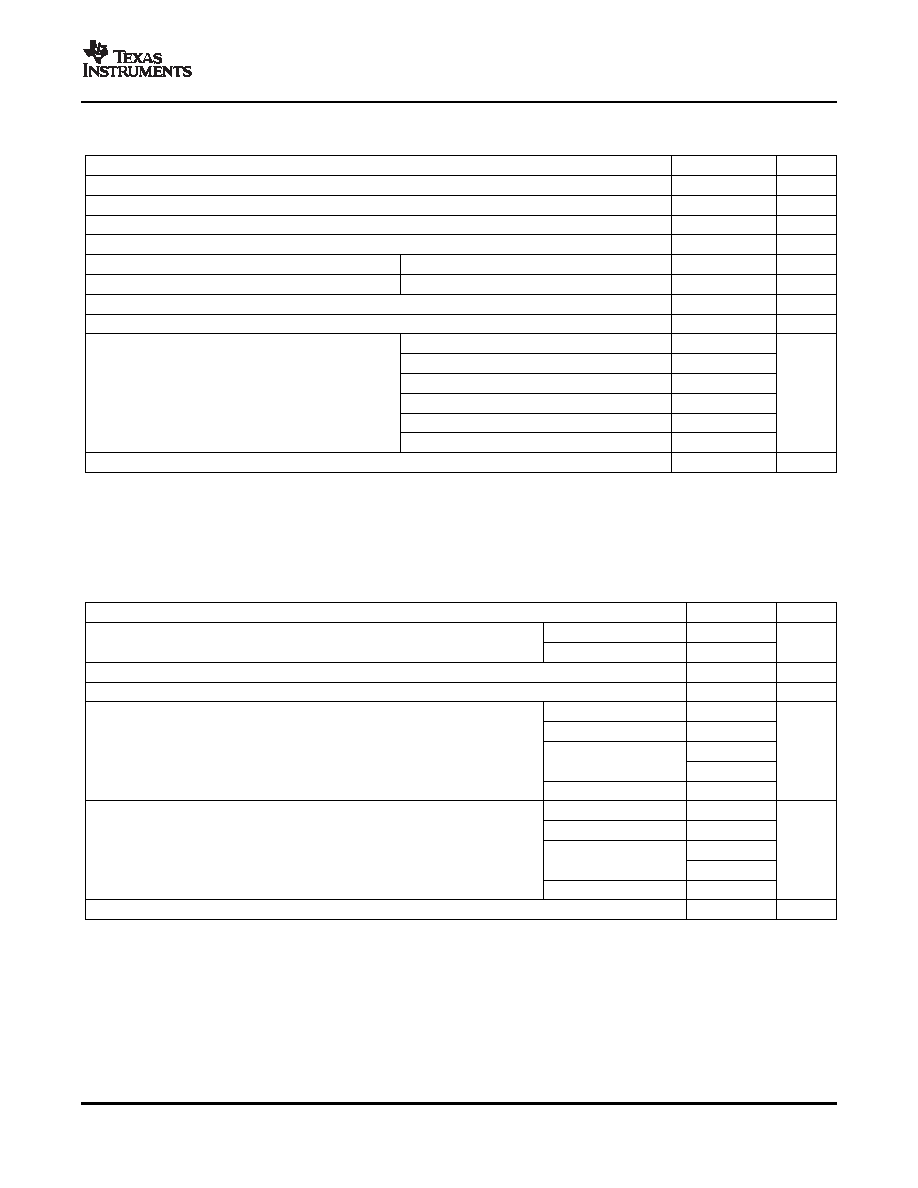
Absolute Maximum Ratings
(1)
Recommended Operating Conditions
(1)
SINGLE SCHMITT-TRIGGER INVERTER
SCES218T – APRIL 1999 – REVISED FEBRUARY 2007
over operating free-air temperature range (unless otherwise noted)
MIN
MAX
UNIT
VCC
Supply voltage range
–0.5
6.5
V
VI
Input voltage range(2)
–0.5
6.5
V
VO
Voltage range applied to any output in the high-impedance or power-off state(2)
–0.5
6.5
V
VO
Voltage range applied to any output in the high or low state(2)(3)
–0.5
VCC + 0.5
V
IIK
Input clamp current
VI < 0
–50
mA
IOK
Output clamp current
VO < 0
–50
mA
IO
Continuous output current
±50
mA
Continuous current through VCC or GND
±100
mA
DBV package
206
DCK package
252
DRL package
142
θ
JA
Package thermal impedance(4)
°C/W
DRY package
234
YZP package
132
YZV package
123
Tstg
Storage temperature range
–65
150
°C
(1)
Stresses beyond those listed under "absolute maximum ratings" may cause permanent damage to the device. These are stress ratings
only, and functional operation of the device at these or any other conditions beyond those indicated under "recommended operating
conditions" is not implied. Exposure to absolute-maximum-rated conditions for extended periods may affect device reliability.
(2)
The input and output negative-voltage ratings may be exceeded if the input and output current ratings are observed.
(3)
The value of VCC is provided in the recommended operating conditions table.
(4)
The package thermal impedance is calculated in accordance with JESD 51-7.
MIN
MAX
UNIT
Operating
1.65
5.5
VCC
Supply voltage
V
Data retention only
1.5
VI
Input voltage
0
5.5
V
VO
Output voltage
0
VCC
V
VCC = 1.65 V
–4
VCC = 2.3 V
–8
IOH
High-level output current
–16
mA
VCC = 3 V
–24
VCC = 4.5 V
–32
VCC = 1.65 V
4
VCC = 2.3 V
8
IOL
Low-level output current
16
mA
VCC = 3 V
24
VCC = 4.5 V
32
TA
Operating free-air temperature
–40
85
°C
(1)
All unused inputs of the device must be held at VCC or GND to ensure proper device operation. Refer to the TI application report,
Implications of Slow or Floating CMOS Inputs, literature number SCBA004.
3
相关PDF资料 |
PDF描述 |
|---|---|
| SN74LVC1G18DCKRG4 | LVC/LCX/Z SERIES, OTHER DECODER/DRIVER, TRUE OUTPUT, PDSO6 |
| SN74LVC1G19DBVR | LVC/LCX/Z SERIES, OTHER DECODER/DRIVER, COMPLEMENTARY OUTPUT, PDSO6 |
| SN74LVC1G29YEPR | LVC/LCX/Z SERIES, OTHER DECODER/DRIVER, INVERTED OUTPUT, BGA8 |
| SN74LVC1G32DRLR | LVC/LCX/Z SERIES, 2-INPUT OR GATE, PDSO5 |
| SN74LVC1G32DBVR | LVC/LCX/Z SERIES, 2-INPUT OR GATE, PDSO5 |
相关代理商/技术参数 |
参数描述 |
|---|---|
| SN74LVC1G14YZVR | 功能描述:变换器 Single Schmitt- Trigger Inverter RoHS:否 制造商:NXP Semiconductors 电路数量:6 逻辑系列:74ABT 逻辑类型:BiCMOS 高电平输出电流:- 15 mA 低电平输出电流:20 mA 传播延迟时间:2.2 ns 电源电压-最大:5.5 V 电源电压-最小:4.5 V 最大工作温度:+ 85 C 最小工作温度:- 40 C 工作温度范围: 封装 / 箱体:DIP-14 封装:Tube |
| SN74LVC1G175DBVR | 功能描述:触发器 Sngl DType Flip Flop RoHS:否 制造商:Texas Instruments 电路数量:2 逻辑系列:SN74 逻辑类型:D-Type Flip-Flop 极性:Inverting, Non-Inverting 输入类型:CMOS 输出类型: 传播延迟时间:4.4 ns 高电平输出电流:- 16 mA 低电平输出电流:16 mA 电源电压-最大:5.5 V 最大工作温度:+ 85 C 安装风格:SMD/SMT 封装 / 箱体:X2SON-8 封装:Reel |
| SN74LVC1G175DBVT | 功能描述:触发器 SNGL DType FlipFlop RoHS:否 制造商:Texas Instruments 电路数量:2 逻辑系列:SN74 逻辑类型:D-Type Flip-Flop 极性:Inverting, Non-Inverting 输入类型:CMOS 输出类型: 传播延迟时间:4.4 ns 高电平输出电流:- 16 mA 低电平输出电流:16 mA 电源电压-最大:5.5 V 最大工作温度:+ 85 C 安装风格:SMD/SMT 封装 / 箱体:X2SON-8 封装:Reel |
| SN74LVC1G175DCKR | 功能描述:触发器 Single D-Type Flip-Flop RoHS:否 制造商:Texas Instruments 电路数量:2 逻辑系列:SN74 逻辑类型:D-Type Flip-Flop 极性:Inverting, Non-Inverting 输入类型:CMOS 输出类型: 传播延迟时间:4.4 ns 高电平输出电流:- 16 mA 低电平输出电流:16 mA 电源电压-最大:5.5 V 最大工作温度:+ 85 C 安装风格:SMD/SMT 封装 / 箱体:X2SON-8 封装:Reel |
| SN74LVC1G175DCKRG4 | 制造商:Texas Instruments 功能描述:TISSN74LVC1G175DCKRG4 SINGLE D-TYPE FLIP |
发布紧急采购,3分钟左右您将得到回复。