- 您现在的位置:买卖IC网 > PDF目录97086 > SN74LVC1G374QDCKRQ1 (TEXAS INSTRUMENTS INC) LVC/LCX/Z SERIES, 1-BIT DRIVER, TRUE OUTPUT, PDSO6 PDF资料下载
参数资料
| 型号: | SN74LVC1G374QDCKRQ1 |
| 厂商: | TEXAS INSTRUMENTS INC |
| 元件分类: | 总线收发器 |
| 英文描述: | LVC/LCX/Z SERIES, 1-BIT DRIVER, TRUE OUTPUT, PDSO6 |
| 封装: | PLASTIC, SC-70, 6 PIN |
| 文件页数: | 1/10页 |
| 文件大小: | 226K |
| 代理商: | SN74LVC1G374QDCKRQ1 |
SN74LVC1G374Q1
SINGLE DTYPE FLIPFLOP
WITH 3STATE OUTPUT
SCES607A SEPTEMBER 2004 REVISED APRIL 2008
1
POST OFFICE BOX 655303
DALLAS, TEXAS 75265
D Qualified for Automotive Applications
D Supports 5-V VCC Operation
D Inputs Accept Voltages to 5.5 V
D Max tpd of 4 ns at 3.3 V
D Low Power Consumption, 10-A Max ICC
D ±24-mA Output Drive at 3.3 V
D Ioff Supports Partial-Power-Down Mode
Operation
D Latch-Up Performance Exceeds 100 mA
Per JESD 78, Class II
D ESD Protection Exceeds JESD 22
2000-V Human-Body Model (A114-A)
200-V Machine Model (A115-A)
1000-V Charged-Device Model (C101)
description/ordering information
This single D-type flip-flop is designed for 1.65-V to
5.5-V VCC operation.
The SN74LVC1G374 features a 3-state output
designed specifically for driving highly capacitive or
relatively low-impedance loads. This device is
particularly suitable for implementing buffer registers,
input/output (I/O) ports, bidirectional bus drivers, and
working registers.
On the positive transition of the clock (CLK) input, the Q output is set to the logic level set up at the data (D)
input.
A buffered output-enable (OE) input can be used to place the output in either a normal logic state (high or low
logic levels) or the high-impedance state. In the high-impedance state, the output neither loads nor drives the
bus lines significantly. The high-impedance state and increased drive provide the capability to drive bus lines
without interface or pullup components.
OE does not affect the internal operations of the flip-flop. Old data can be retained or new data can be entered
while the outputs are in the high-impedance state.
To ensure the high-impedance state during power up or power down, OE should be tied to VCC through a pullup
resistor; the minimum value of the resistor is determined by the current-sinking capability of the driver.
This device is fully specified for partial-power-down applications using Ioff. The Ioff circuitry disables the outputs,
preventing damaging current backflow through the device when it is powered down.
ORDERING INFORMATION{
TA
PACKAGE}
ORDERABLE
PART NUMBER
TOP-SIDE
MARKING§
40
°C to 125°C
SOT (SOT-23) DBV
Reel of 3000
SN74LVC1G374QDBVRQ1
CA40
40
°C to 125°C
SOT (SC-70) DCK
Reel of 3000
SN74LVC1G374QDCKRQ1
D40
For the most current package and ordering information, see the Package Option Addendum at the end of this document, or see
the TI web site at http://www.ti.com.
}Package drawings, thermal data, and symbolization are available at http://www.ti.com/packaging.
§ DBV/DCK: The actual top-side marking has one additional character that designates the wafer fab/assembly site.
Copyright
2008, Texas Instruments Incorporated
Please be aware that an important notice concerning availability, standard warranty, and use in critical applications of
Texas Instruments semiconductor products and disclaimers thereto appears at the end of this data sheet.
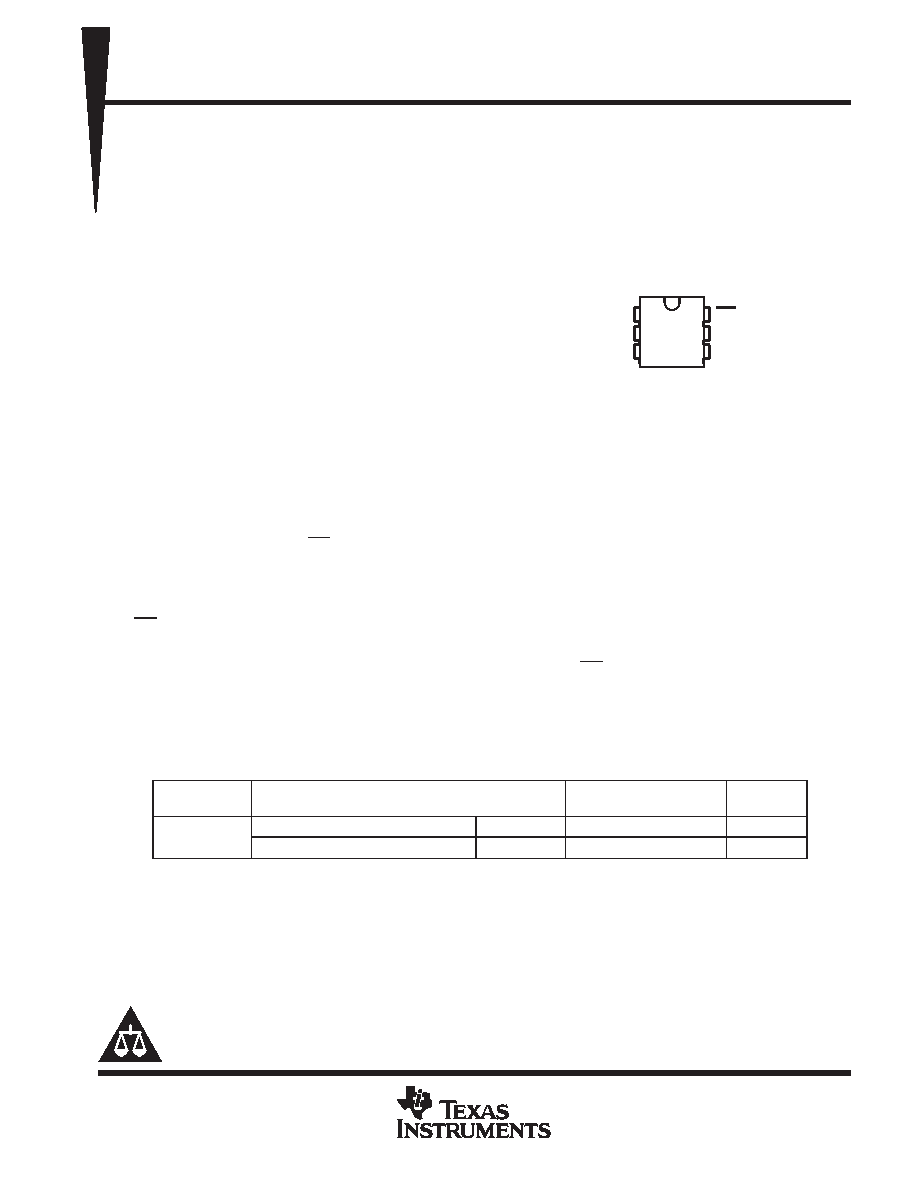
DBV OR DCK PACKAGE
(TOP VIEW)
1
2
3
6
5
4
CLK
GND
D
OE
VCC
Q
PRODUCTION DATA information is current as of publication date.
Products conform to specifications per the terms of Texas Instruments
standard warranty. Production processing does not necessarily include
testing of all parameters.
相关PDF资料 |
PDF描述 |
|---|---|
| SN74LVC1G80DCK | LVC/LCX/Z SERIES, POSITIVE EDGE TRIGGERED D FLIP-FLOP, INVERTED OUTPUT, PDSO5 |
| SN74LVC1G86DCK | LVC/LCX/Z SERIES, 2-INPUT XOR GATE, PDSO5 |
| SN74LVC1GU04ADBVR | LVC/LCX/Z SERIES, 1-INPUT INVERT GATE, PDSO5 |
| SN74LVC1GU04ADCK | LVC/LCX/Z SERIES, 1-INPUT INVERT GATE, PDSO5 |
| SN74LVC241ADW | LVC/LCX/Z SERIES, DUAL 4-BIT DRIVER, TRUE OUTPUT, PDSO20 |
相关代理商/技术参数 |
参数描述 |
|---|---|
| SN74LVC1G374YEPR | 功能描述:IC D-TYPE LATCH SGL 3-ST 6DSBGA RoHS:是 类别:集成电路 (IC) >> 逻辑 - 锁销 系列:74LVC 产品变化通告:Product Discontinuation 09/Dec/2010 标准包装:1,500 系列:74VCX 逻辑类型:D 型透明锁存器 电路:8:8 输出类型:三态 电源电压:1.8 V ~ 3.6 V 独立电路:2 延迟时间 - 传输:1.5ns 输出电流高,低:6mA,6mA 工作温度:-40°C ~ 85°C 安装类型:表面贴装 封装/外壳:48-TFSOP(0.240",6.10mm 宽) 供应商设备封装:48-TSSOP 包装:带卷 (TR) |
| SN74LVC1G374YZPR | 功能描述:触发器 SnglDTypeFlipFlop RoHS:否 制造商:Texas Instruments 电路数量:2 逻辑系列:SN74 逻辑类型:D-Type Flip-Flop 极性:Inverting, Non-Inverting 输入类型:CMOS 输出类型: 传播延迟时间:4.4 ns 高电平输出电流:- 16 mA 低电平输出电流:16 mA 电源电压-最大:5.5 V 最大工作温度:+ 85 C 安装风格:SMD/SMT 封装 / 箱体:X2SON-8 封装:Reel |
| SN74LVC1G386DBVR | 功能描述:逻辑门 Sngl 3 Inp t+ XOR Gt RoHS:否 制造商:Texas Instruments 产品:OR 逻辑系列:LVC 栅极数量:2 线路数量(输入/输出):2 / 1 高电平输出电流:- 16 mA 低电平输出电流:16 mA 传播延迟时间:3.8 ns 电源电压-最大:5.5 V 电源电压-最小:1.65 V 最大工作温度:+ 125 C 安装风格:SMD/SMT 封装 / 箱体:DCU-8 封装:Reel |
| SN74LVC1G386DCKR | 功能描述:逻辑门 SINGLE 3-INPUT Pos- XOR GATE RoHS:否 制造商:Texas Instruments 产品:OR 逻辑系列:LVC 栅极数量:2 线路数量(输入/输出):2 / 1 高电平输出电流:- 16 mA 低电平输出电流:16 mA 传播延迟时间:3.8 ns 电源电压-最大:5.5 V 电源电压-最小:1.65 V 最大工作温度:+ 125 C 安装风格:SMD/SMT 封装 / 箱体:DCU-8 封装:Reel |
| SN74LVC1G386DRYR | 功能描述:逻辑门 Sgl 3-Inp Pos-XOR Gate RoHS:否 制造商:Texas Instruments 产品:OR 逻辑系列:LVC 栅极数量:2 线路数量(输入/输出):2 / 1 高电平输出电流:- 16 mA 低电平输出电流:16 mA 传播延迟时间:3.8 ns 电源电压-最大:5.5 V 电源电压-最小:1.65 V 最大工作温度:+ 125 C 安装风格:SMD/SMT 封装 / 箱体:DCU-8 封装:Reel |
发布紧急采购,3分钟左右您将得到回复。