- 您现在的位置:买卖IC网 > PDF目录98125 > SN74LVC540ADBRE4 (TEXAS INSTRUMENTS INC) LVC/LCX/Z SERIES, 8-BIT DRIVER, INVERTED OUTPUT, PDSO20 PDF资料下载
参数资料
| 型号: | SN74LVC540ADBRE4 |
| 厂商: | TEXAS INSTRUMENTS INC |
| 元件分类: | 总线收发器 |
| 英文描述: | LVC/LCX/Z SERIES, 8-BIT DRIVER, INVERTED OUTPUT, PDSO20 |
| 封装: | GREEN, PLASTIC, SSOP-20 |
| 文件页数: | 14/20页 |
| 文件大小: | 682K |
| 代理商: | SN74LVC540ADBRE4 |
www.ti.com
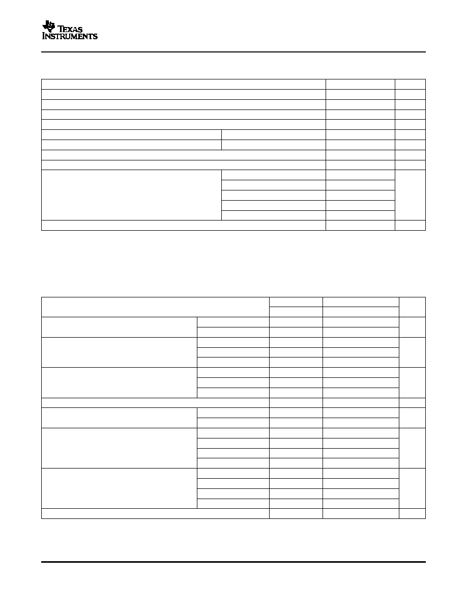
Absolute Maximum Ratings
(1)
Recommended Operating Conditions
(1)
SN54LVC540A, SN74LVC540A
OCTAL BUFFERS/DRIVERS
WITH 3-STATE OUTPUTS
SCAS297M – JANUARY 1993 – REVISED MAY 2005
over operating free-air temperature range (unless otherwise noted)
MIN
MAX
UNIT
VCC
Supply voltage range
–0.5
6.5
V
VI
Input voltage range(2)
–0.5
6.5
V
VO
Voltage range applied to any output in the high-impedance or power-off state(2)
–0.5
6.5
V
VO
Voltage range applied to any output in the high or low state(2)(3)
–0.5
VCC + 0.5
V
IIK
Input clamp current
VI < 0
–50
mA
IOK
Output clamp current
VO < 0
–50
mA
IO
Continuous output current
±50
mA
Continuous current through VCC or GND
±100
mA
DB package
70
DGV package
92
θ
JA
Package thermal impedance(4)
DW package
58
°C/W
NS package
60
PW package
83
Tstg
Storage temperature range
–65
150
°C
(1)
Stresses beyond those listed under "absolute maximum ratings" may cause permanent damage to the device. These are stress ratings
only, and functional operation of the device at these or any other conditions beyond those indicated under "recommended operating
conditions" is not implied. Exposure to absolute-maximum-rated conditions for extended periods may affect device reliability.
(2)
The input negative-voltage and output voltage ratings may be exceeded if the input and output current ratings are observed.
(3)
The value of VCC is provided in the recommended operating conditions table.
(4)
The package thermal impedance is calculated in accordance with JESD 51-7.
SN54LVC540A
SN74LVC540A
UNIT
MIN
MAX
MIN
MAX
Operating
2
3.6
1.65
3.6
VCC
Supply voltage
V
Data retention only
1.5
VCC = 1.65 V to 1.95 V
0.65 × VCC
VIH
High-level input voltage
VCC = 2.3 V to 2.7 V
1.7
V
VCC = 2.7 V to 3.6 V
2
VCC = 1.65 V to 1.95 V
0.35 × VCC
VIL
Low-level input voltage
VCC = 2.3 V to 2.7 V
0.7
V
VCC = 2.7 V to 3.6 V
0.8
VI
Input voltage
0
5.5
0
5.5
V
High or low state
0
VCC
0
VCC
VO
Output voltage
V
3-state
0
5.5
0
5.5
VCC = 1.65 V
–4
VCC = 2.3 V
–8
IOH
High-level output current
mA
VCC = 2.7 V
–12
VCC = 3 V
–24
VCC = 1.65 V
4
VCC = 2.3 V
8
IOL
Low-level output current
mA
VCC = 2.7 V
12
VCC = 3 V
24
TA
Operating free-air temperature
–55
125
–40
85
°C
(1)
All unused inputs of the device must be held at VCC or GND to ensure proper device operation. Refer to the TI application report,
Implications of Slow or Floating CMOS Inputs, literature number SCBA004.
3
相关PDF资料 |
PDF描述 |
|---|---|
| SN74LVC541APWRG3 | LVC/LCX/Z SERIES, 8-BIT DRIVER, TRUE OUTPUT, PDSO20 |
| SN74LVC543ADWE4 | LVC/LCX/Z SERIES, 8-BIT REGISTERED TRANSCEIVER, TRUE OUTPUT, PDSO24 |
| SN74LVC543APWG4 | LVC/LCX/Z SERIES, 8-BIT REGISTERED TRANSCEIVER, TRUE OUTPUT, PDSO24 |
| SN74LVC574ADWG4 | LVC/LCX/Z SERIES, 8-BIT DRIVER, TRUE OUTPUT, PDSO20 |
| SNJ54LVC574AW | LVC/LCX/Z SERIES, 8-BIT DRIVER, TRUE OUTPUT, CDFP16 |
相关代理商/技术参数 |
参数描述 |
|---|---|
| SN74LVC540ADBRG4 | 功能描述:缓冲器和线路驱动器 Octal Buffer Driver RoHS:否 制造商:Micrel 输入线路数量:1 输出线路数量:2 极性:Non-Inverting 电源电压-最大:+/- 5.5 V 电源电压-最小:+/- 2.37 V 最大工作温度:+ 85 C 安装风格:SMD/SMT 封装 / 箱体:MSOP-8 封装:Reel |
| SN74LVC540ADGVR | 功能描述:缓冲器和线路驱动器 Tri-State Octal RoHS:否 制造商:Micrel 输入线路数量:1 输出线路数量:2 极性:Non-Inverting 电源电压-最大:+/- 5.5 V 电源电压-最小:+/- 2.37 V 最大工作温度:+ 85 C 安装风格:SMD/SMT 封装 / 箱体:MSOP-8 封装:Reel |
| SN74LVC540ADGVRE4 | 功能描述:缓冲器和线路驱动器 OCTAL FET BUS SWITCH RoHS:否 制造商:Micrel 输入线路数量:1 输出线路数量:2 极性:Non-Inverting 电源电压-最大:+/- 5.5 V 电源电压-最小:+/- 2.37 V 最大工作温度:+ 85 C 安装风格:SMD/SMT 封装 / 箱体:MSOP-8 封装:Reel |
| SN74LVC540ADGVRG4 | 功能描述:缓冲器和线路驱动器 Octal Buffer Driver RoHS:否 制造商:Micrel 输入线路数量:1 输出线路数量:2 极性:Non-Inverting 电源电压-最大:+/- 5.5 V 电源电压-最小:+/- 2.37 V 最大工作温度:+ 85 C 安装风格:SMD/SMT 封装 / 箱体:MSOP-8 封装:Reel |
| SN74LVC540ADW | 功能描述:缓冲器和线路驱动器 Tri-State Octal RoHS:否 制造商:Micrel 输入线路数量:1 输出线路数量:2 极性:Non-Inverting 电源电压-最大:+/- 5.5 V 电源电压-最小:+/- 2.37 V 最大工作温度:+ 85 C 安装风格:SMD/SMT 封装 / 箱体:MSOP-8 封装:Reel |
发布紧急采购,3分钟左右您将得到回复。