- 您现在的位置:买卖IC网 > PDF目录373480 > SN74LVCH16241 (Texas Instruments, Inc.) 16-Bit Buffers/Drivers With 3-State Outputs(16位缓冲器/驱动器(三态输出)) PDF资料下载
参数资料
| 型号: | SN74LVCH16241 |
| 厂商: | Texas Instruments, Inc. |
| 英文描述: | 16-Bit Buffers/Drivers With 3-State Outputs(16位缓冲器/驱动器(三态输出)) |
| 中文描述: | 16位缓冲器/驱动器与3态输出(16位缓冲器/驱动器(三态输出)) |
| 文件页数: | 3/5页 |
| 文件大小: | 98K |
| 代理商: | SN74LVCH16241 |
SN74LVCH16241A
16-BIT BUFFER/DRIVER
WITH 3-STATE OUTPUTS
SCAS348C – MARCH 1994 – REVISED JANUARY 1997
3
POST OFFICE BOX 655303
DALLAS, TEXAS 75265
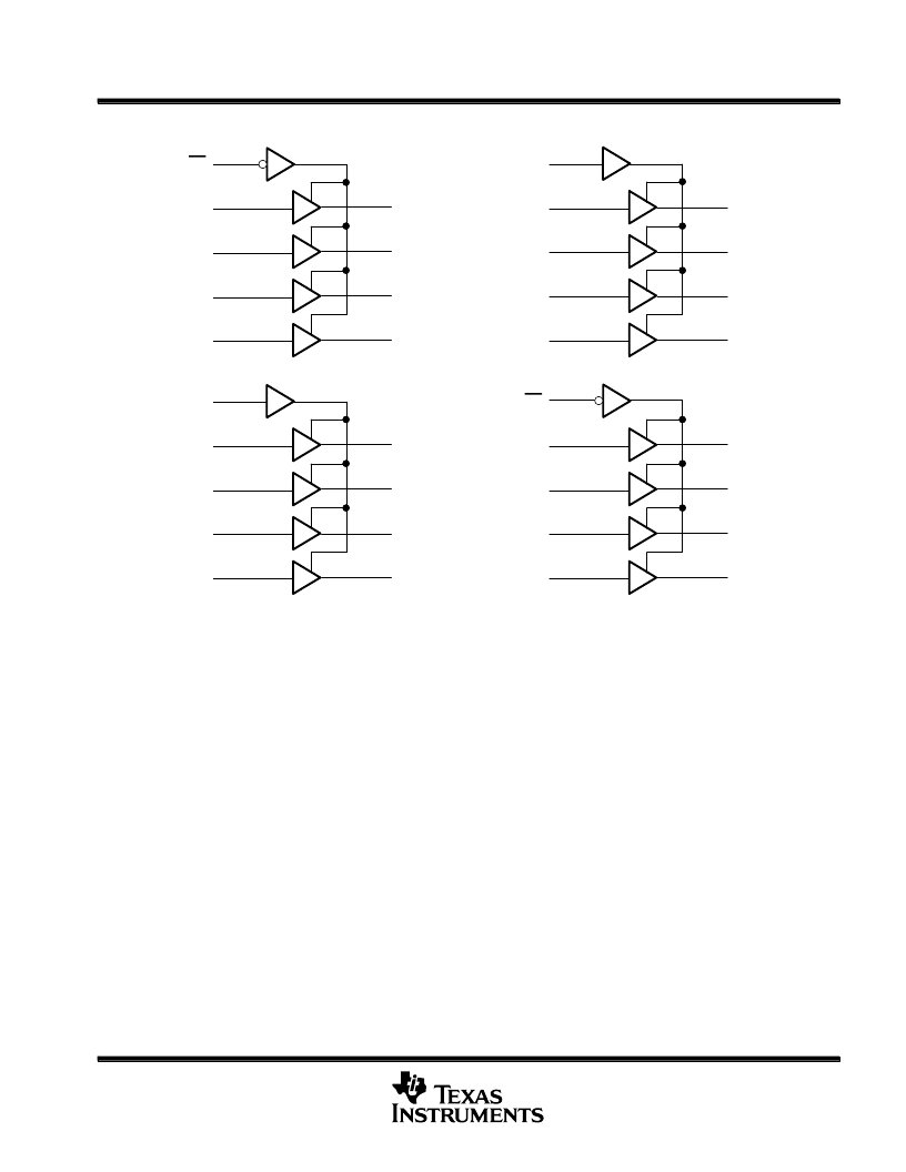
logic diagram (positive logic)
1OE
1
1A1
1A2
1A3
1A4
47
46
44
43
1Y1
1Y2
1Y3
1Y4
2
3
5
6
2OE
48
2A1
2A2
2A3
2A4
41
40
38
37
2Y1
2Y2
2Y3
2Y4
8
9
11
12
3OE
25
3A1
3A2
3A3
3A4
36
35
33
32
3Y1
3Y2
3Y3
3Y4
13
14
16
17
4OE
24
4A1
4A2
4A3
4A4
30
29
27
26
4Y1
4Y2
4Y3
4Y4
19
20
22
23
absolute maximum ratings over operating free-air temperature range (unless otherwise noted)
Supply voltage range, V
CC
Input voltage range, V
I
Voltage range applied to any output in the high-impedance or power-off state, V
O
(see Note 1)
. . . . . . . . . . . . . . . . . . . . . . . . . . . . . . . . . . . . . . . . . . . . . . . . . . . . . . . . . . . . . . . . . . .
Voltage range applied to any output in the high or low state, V
O
(see Notes 1 and 2)
. . . . . . . . . . . . . . . . . . . . . . . . . . . . . . . . . . . . . . . . . . . . . . . . . . . . . . .
Input clamp current, I
IK
(V
I
< 0)
. . . . . . . . . . . . . . . . . . . . . . . . . . . . . . . . . . . . . . . . . . . . . . . . . . . . . . . . . . .
Output clamp current, I
OK
(V
O
< 0 or V
O
> V
CC
)
Continuous output current, I
O
(V
O
= 0 to V
CC
) (see Note 2)
Continuous current through V
CC
or GND
. . . . . . . . . . . . . . . . . . . . . . . . . . . . . . . . . . . . . . . . . . . . . . . . . .
Package thermal impedance,
θ
JA
(see Note 3): DGG package
DL package
Storage temperature range, T
stg
. . . . . . . . . . . . . . . . . . . . . . . . . . . . . . . . . . . . . . . . . . . . . . . . . . .
Stresses beyond those listed under “absolute maximum ratings” may cause permanent damage to the device. These are stress ratings only, and
functional operation of the device at these or any other conditions beyond those indicated under “recommended operating conditions” is not
implied. Exposure to absolute-maximum-rated conditions for extended periods may affect device reliability.
NOTES:
1. The input and output negative-voltage ratings may be exceeded if the input and output clamp-current ratings are observed.
2. The value of VCC is provided in the recommended operating conditions table.
3. The package thermal impedance is calculated in accordance with EIA/JEDEC Std JESD51.
–0.5 V to 6.5 V
–0.5 V to 6.5 V
. . . . . . . . . . . . . . . . . . . . . . . . . . . . . . . . . . . . . . . . . . . . . . . . . . . . . . . . .
. . . . . . . . . . . . . . . . . . . . . . . . . . . . . . . . . . . . . . . . . . . . . . . . . . . . . . . . . . . . .
–0.5 V to 6.5 V
–0.5 V to V
CC
+ 0.5 V
–50 mA
±
50 mA
±
50 mA
±
100 mA
89
°
C/W
94
°
C/W
. . . . . . . . . . . . . . . . . . . . . . . . . . . . . . . . . . . . . . . . . . . .
. . . . . . . . . . . . . . . . . . . . . . . . . . . . . . . . . .
. . . . . . . . . . . . . . . . . . . . . . . . . . . . . . .
. . . . . . . . . . . . . . . . . . . . . . . . . . . . . . . . .
–65
°
C to 150
°
C
P
相关PDF资料 |
PDF描述 |
|---|---|
| SN74LVCH16260 | 12-BIT TO 24-BIT MULTIPLEXED D-TYPE LATCH(12-24多重D锁存器(三态输出)) |
| SN74LVCH16374AGRDR | 16-BIT EDGE-TRIGGERED D-TYPE FLIP-FLOP WITH 3-STATE OUTPUTS |
| SN74LVCH16540 | 16-Bit Buffers/Drivers With 3-State Outputs(16位缓冲器/驱动器(三态输出)) |
| SN74LVCH16541 | 16-Bit Buffers/Drivers With 3-State Outputs(16位缓冲器/驱动器(三态输出)) |
| SN74LVCH16544 | 16-Bit Registered Transceivers(16位记录收发器(三态输出)) |
相关代理商/技术参数 |
参数描述 |
|---|---|
| SN74LVCH16244ADGG | 制造商:Rochester Electronics LLC 功能描述:- Bulk |
| SN74LVCH16244ADGGR | 功能描述:缓冲器和线路驱动器 Tri-State 16-Bit RoHS:否 制造商:Micrel 输入线路数量:1 输出线路数量:2 极性:Non-Inverting 电源电压-最大:+/- 5.5 V 电源电压-最小:+/- 2.37 V 最大工作温度:+ 85 C 安装风格:SMD/SMT 封装 / 箱体:MSOP-8 封装:Reel |
| SN74LVCH16244ADGGRG4 | 制造商:Texas Instruments 功能描述: |
| SN74LVCH16244ADGVR | 功能描述:缓冲器和线路驱动器 Tri-State 16-Bit RoHS:否 制造商:Micrel 输入线路数量:1 输出线路数量:2 极性:Non-Inverting 电源电压-最大:+/- 5.5 V 电源电压-最小:+/- 2.37 V 最大工作温度:+ 85 C 安装风格:SMD/SMT 封装 / 箱体:MSOP-8 封装:Reel |
| SN74LVCH16244ADL | 功能描述:缓冲器和线路驱动器 Tri-State 16-Bit RoHS:否 制造商:Micrel 输入线路数量:1 输出线路数量:2 极性:Non-Inverting 电源电压-最大:+/- 5.5 V 电源电压-最小:+/- 2.37 V 最大工作温度:+ 85 C 安装风格:SMD/SMT 封装 / 箱体:MSOP-8 封装:Reel |
发布紧急采购,3分钟左右您将得到回复。