- 您现在的位置:买卖IC网 > PDF目录373480 > SN74LVCH16260 (Texas Instruments, Inc.) 12-BIT TO 24-BIT MULTIPLEXED D-TYPE LATCH(12-24多重D锁存器(三态输出)) PDF资料下载
参数资料
| 型号: | SN74LVCH16260 |
| 厂商: | Texas Instruments, Inc. |
| 英文描述: | 12-BIT TO 24-BIT MULTIPLEXED D-TYPE LATCH(12-24多重D锁存器(三态输出)) |
| 中文描述: | 12位至24位复用D型锁存器(12-24多重?锁存器(三态输出)) |
| 文件页数: | 4/9页 |
| 文件大小: | 198K |
| 代理商: | SN74LVCH16260 |
SN74ALVCH162260
12-BIT TO 24-BIT MULTIPLEXED D-TYPE LATCH
WITH 3-STATE OUTPUTS
SCAS570B – MARCH 1996 – REVISED NOVEMBER 1996
4
POST OFFICE BOX 655303
DALLAS, TEXAS 75265
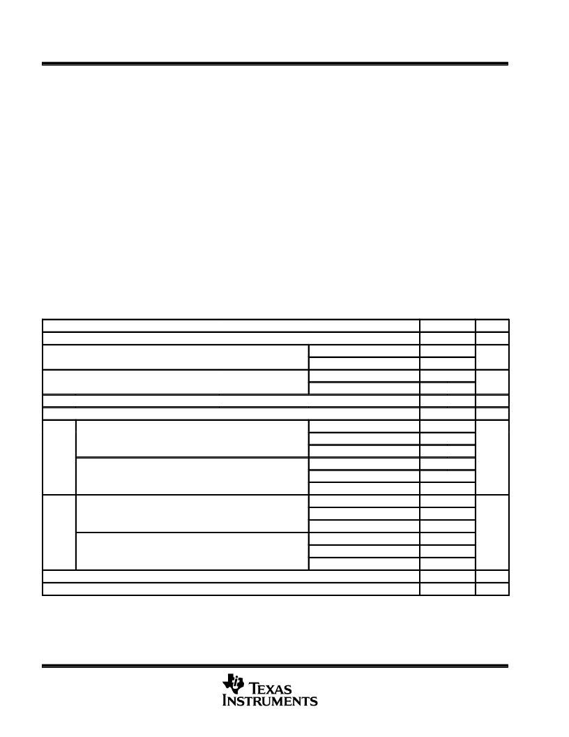
absolute maximum ratings over operating free-air temperature range (unless otherwise noted)
Supply voltage range, V
CC
Input voltage range, V
I
: Except I/O ports (see Note 1)
I/O ports (see Notes 1 and 2)
Output voltage range, V
O
(see Notes 1 and 2)
Input clamp current, I
IK
(V
I
< 0)
Output clamp current, I
OK
(V
O
< 0 or V
O
> V
CC
)
Continuous output current, I
O
(V
O
= 0 to V
CC
)
Continuous current through each V
CC
or GND
Maximum power dissipation at T
A
= 55
°
C (in still air) (see Note 3):DGG package
–0.5 V to
4.6 V
–0.5 V to 4.6 V
–0.5 V to V
CC
+ 0.5 V
–0.5 V to V
CC
+ 0.5 V
. . . . . . . . . . . . . . . . . . . . . . . . . . . . . . . . . . . . . . . . . . . . . . . . . . . . . . . . .
. . . . . . . . . . . . . . . . . . . . . . . . . . . . . . . . .
. . . . . . . . . . . . . . . . . . . . . . . . . .
. . . . . . . . . . . . . . . . . . . . . . . . . . . . . . . . .
. . . . . . . . . . . . . . . . . . . . . . . . . . . . . . . . . . . . . . . . . . . . . . . . . . . . . . . . . . .
. . . . . . . . . . . . . . . . . . . . . . . . . . . . . . . . . . . . . . . . . . . .
. . . . . . . . . . . . . . . . . . . . . . . . . . . . . . . . . . . . . . . . . . . . . .
. . . . . . . . . . . . . . . . . . . . . . . . . . . . . . . . . . . . . . . . . . . . .
–50 mA
±
50 mA
±
50 mA
±
100 mA
1 W
1.4 W
. . . . . . . . . . . . . . . . . .
. . . . . . . . . . . . . . . . . . .
DL package
Storage temperature range, T
stg
Stresses beyond those listed under “absolute maximum ratings” may cause permanent damage to the device. These are stress ratings only, and
functional operation of the device at these or any other conditions beyond those indicated under “recommended operating conditions” is not
implied. Exposure to absolute-maximum-rated conditions for extended periods may affect device reliability.
NOTES:
1. The input and output negative-voltage ratings may be exceeded if the input and output clamp-current ratings are observed.
2. This value is limited to 4.6 V maximum.
3. The maximum package power dissipation is calculated using a junction temperature of 150
°
C and a board trace length of 750 mils.
For more information, refer to the Package Thermal Considerationsapplication note in the ABT Advanced BiCMOS Technology Data
Book
–65
°
C to 150
°
C
. . . . . . . . . . . . . . . . . . . . . . . . . . . . . . . . . . . . . . . . . . . . . . . . . . .
recommended operating conditions (see Note 4)
MIN
MAX
UNIT
VCC
Supply voltage
2.3
3.6
V
VIH
High-level input voltage
VCC = 2.3 V to 2.7 V
VCC = 2.7 V to 3.6 V
VCC = 2.3 V to 2.7 V
VCC = 2.7 V to 3.6 V
1.7
V
2
VIL
Low-level input voltage
0.7
V
0.8
VI
VO
Input voltage
0
VCC
VCC
–12
V
Output voltage
0
V
IOH
Hi h l
g
p
l
(A
)
VCC = 2.3 V
VCC = 2.7 V
VCC = 3 V
VCC = 2.3 V
VCC = 2.7 V
VCC = 3 V
VCC = 2.3 V
VCC = 2.7 V
VCC = 3 V
VCC = 2.3 V
VCC = 2.7 V
VCC = 3 V
–12
p
–24
mA
Hi h l
High-level output current (B port)
–6
–8
–12
IOL
Low-level output current (A port)
12
12
24
mA
Low-level output current (B port)
6
8
12
t/
v
TA
NOTE 4: Unused control inputs must be held high or low to prevent them from floating.
Input transition rise or fall rate
0
10
ns/V
°
C
Operating free-air temperature
–40
85
相关PDF资料 |
PDF描述 |
|---|---|
| SN74LVCH16374AGRDR | 16-BIT EDGE-TRIGGERED D-TYPE FLIP-FLOP WITH 3-STATE OUTPUTS |
| SN74LVCH16540 | 16-Bit Buffers/Drivers With 3-State Outputs(16位缓冲器/驱动器(三态输出)) |
| SN74LVCH16541 | 16-Bit Buffers/Drivers With 3-State Outputs(16位缓冲器/驱动器(三态输出)) |
| SN74LVCH16544 | 16-Bit Registered Transceivers(16位记录收发器(三态输出)) |
| SN74LVCH16T245GQLR | 16-BIT DUAL-SUPPLY BUS TRANSCEIVER WITH CONFIGURABLE VOLTAGE TRANSLATION AND 3-STATE OUTPUTS |
相关代理商/技术参数 |
参数描述 |
|---|---|
| SN74LVCH16270DGGR | 制造商:Texas Instruments 功能描述: |
| SN74LVCH16373ADGGR | 功能描述:闭锁 Tri-St. 16bit D-Type RoHS:否 制造商:Micrel 电路数量:1 逻辑类型:CMOS 逻辑系列:TTL 极性:Non-Inverting 输出线路数量:9 高电平输出电流: 低电平输出电流: 传播延迟时间: 电源电压-最大:12 V 电源电压-最小:5 V 最大工作温度:+ 85 C 最小工作温度:- 40 C 封装 / 箱体:SOIC-16 封装:Reel |
| SN74LVCH16373ADGVR | 功能描述:闭锁 Tri-St. 16bit D-Type RoHS:否 制造商:Micrel 电路数量:1 逻辑类型:CMOS 逻辑系列:TTL 极性:Non-Inverting 输出线路数量:9 高电平输出电流: 低电平输出电流: 传播延迟时间: 电源电压-最大:12 V 电源电压-最小:5 V 最大工作温度:+ 85 C 最小工作温度:- 40 C 封装 / 箱体:SOIC-16 封装:Reel |
| SN74LVCH16373ADL | 功能描述:闭锁 Tri-St. 16bit D-Type RoHS:否 制造商:Micrel 电路数量:1 逻辑类型:CMOS 逻辑系列:TTL 极性:Non-Inverting 输出线路数量:9 高电平输出电流: 低电平输出电流: 传播延迟时间: 电源电压-最大:12 V 电源电压-最小:5 V 最大工作温度:+ 85 C 最小工作温度:- 40 C 封装 / 箱体:SOIC-16 封装:Reel |
| SN74LVCH16373ADLG4 | 功能描述:闭锁 Tri-St. 16bit D-Type RoHS:否 制造商:Micrel 电路数量:1 逻辑类型:CMOS 逻辑系列:TTL 极性:Non-Inverting 输出线路数量:9 高电平输出电流: 低电平输出电流: 传播延迟时间: 电源电压-最大:12 V 电源电压-最小:5 V 最大工作温度:+ 85 C 最小工作温度:- 40 C 封装 / 箱体:SOIC-16 封装:Reel |
发布紧急采购,3分钟左右您将得到回复。