- 您现在的位置:买卖IC网 > PDF目录373480 > SN74LVCH16540 (Texas Instruments, Inc.) 16-Bit Buffers/Drivers With 3-State Outputs(16位缓冲器/驱动器(三态输出)) PDF资料下载
参数资料
| 型号: | SN74LVCH16540 |
| 厂商: | Texas Instruments, Inc. |
| 英文描述: | 16-Bit Buffers/Drivers With 3-State Outputs(16位缓冲器/驱动器(三态输出)) |
| 中文描述: | 16位缓冲器/驱动器与3态输出(16位缓冲器/驱动器(三态输出)) |
| 文件页数: | 2/4页 |
| 文件大小: | 82K |
| 代理商: | SN74LVCH16540 |
SN74LVC16540
16-BIT BUFFER/DRIVER
WITH 3-STATE OUTPUTS
SCAS349A – MARCH 1994 – REVISED JULY 1995
2
POST OFFICE BOX 655303
DALLAS, TEXAS 75265
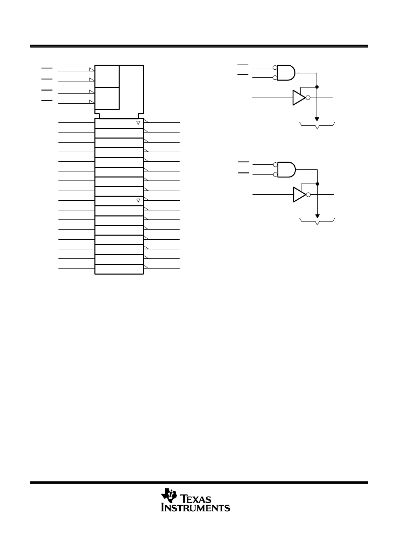
logic symbol
logic diagram (positive logic)
1
48
25
24
1OE1
1OE2
2OE1
2OE2
1A1
47
2
1Y1
36
13
2Y1
2A1
To Seven Other Channels
To Seven Other Channels
47
1A1
1
1Y1
2
48
46
1A2
1Y2
3
24
25
44
1A3
1Y3
5
43
1A4
1Y4
6
41
1A5
1Y5
8
40
1A6
1Y6
9
38
1A7
1Y7
11
37
1A8
1Y8
12
&
&
EN2
EN1
1
1
36
2A1
2Y1
13
35
2A2
2Y2
14
33
2A3
2Y3
16
32
2A4
2Y4
17
30
2A5
2Y5
19
29
2A6
2Y6
20
27
2A7
2Y7
22
26
2A8
2Y8
23
1
2
1OE1
1OE2
2OE1
2OE2
This symbol is in accordance with ANSI/IEEE Std 91-1984 and
IEC Publication 617-12.
absolute maximum ratings over operating free-air temperature range (unless otherwise noted)
Supply voltage range, V
CC
Input voltage range, V
I
Voltage range applied to any output in the high-impedance state
or power-off state, V
O
(see Note 1)
Voltage range applied to any output in the high or low state,
V
O
(see Notes 1 and 2)
. . . . . . . . . . . . . . . . . . . . . . . . . . . . . . . . . . . . . . . . . . . . . . . . . . . .
Input clamp current, I
IK
(V
I
< 0)
. . . . . . . . . . . . . . . . . . . . . . . . . . . . . . . . . . . . . . . . . . . . . . . . . . . . . . . . . .
Output clamp current, I
OK
(V
O
< 0 or V
O
> V
CC
)
Continuous output current, I
O
(V
O
= 0 to V
CC
)
. . . . . . . . . . . . . . . . . . . . . . . . . . . . . . . . . . . . . . . . . . . . .
Continuous current through V
CC
or GND
. . . . . . . . . . . . . . . . . . . . . . . . . . . . . . . . . . . . . . . . . . . . . . . . .
Maximum power dissipation at T
A
= 55
°
C (in still air) (see Note 3):DGG package
–0.5 V to 6.5 V
–0.5 V to 6.5 V
. . . . . . . . . . . . . . . . . . . . . . . . . . . . . . . . . . . . . . . . . . . . . . . . . . . . . . . .
. . . . . . . . . . . . . . . . . . . . . . . . . . . . . . . . . . . . . . . . . . . . . . . . . . . . . . . . . . . .
–0.5 V to 6.5 V
. . . . . . . . . . . . . . . . . . . . . . . . . . . . . . . . . . . . . . . . . . . . . . .
–0.5 V to V
CC
+ 0.5 V
–50 mA
±
50 mA
±
50 mA
±
100 mA
0.85 W
1.2 W
. . . . . . . . . . . . . . . . . . . . . . . . . . . . . . . . . . . . . . . . . . .
. . . . . . . . . . . . . . .
. . . . . . . . . . . . . . . . . .
DL package
Storage temperature range, T
stg
Stresses beyond those listed under “absolute maximum ratings” may cause permanent damage to the device. These are stress ratings only, and
functional operation of the device at these or any other conditions beyond those indicated under “recommended operating conditions” is not
implied. Exposure to absolute-maximum-rated conditions for extended periods may affect device reliability.
NOTES:
1. The input and output negative-voltage ratings may be exceeded if the input and output clamp-current ratings are observed.
2. This value is limited to 4.6 V maximum.
3. The maximum package power dissipation is calculated using a junction temperature of 150
°
C and a board trace length of 750 mils.
For more information, refer to the Package Thermal Considerationsapplication note in the 1994 ABT Advanced BiCMOS Technology
Data Book literature number SCBD002B.
–65
°
C to 150
°
C
. . . . . . . . . . . . . . . . . . . . . . . . . . . . . . . . . . . . . . . . . . . . . . . . . .
P
相关PDF资料 |
PDF描述 |
|---|---|
| SN74LVCH16541 | 16-Bit Buffers/Drivers With 3-State Outputs(16位缓冲器/驱动器(三态输出)) |
| SN74LVCH16544 | 16-Bit Registered Transceivers(16位记录收发器(三态输出)) |
| SN74LVCH16T245GQLR | 16-BIT DUAL-SUPPLY BUS TRANSCEIVER WITH CONFIGURABLE VOLTAGE TRANSLATION AND 3-STATE OUTPUTS |
| SN74LVCH16T245ZQLR | 16-BIT DUAL-SUPPLY BUS TRANSCEIVER WITH CONFIGURABLE VOLTAGE TRANSLATION AND 3-STATE OUTPUTS |
| SN74LVCR162245DGG | 12-Bit Asynchronous Binary Counters 16-SOIC -40 to 85 |
相关代理商/技术参数 |
参数描述 |
|---|---|
| SN74LVCH16540ADGGR | 功能描述:缓冲器和线路驱动器 16bit RoHS:否 制造商:Micrel 输入线路数量:1 输出线路数量:2 极性:Non-Inverting 电源电压-最大:+/- 5.5 V 电源电压-最小:+/- 2.37 V 最大工作温度:+ 85 C 安装风格:SMD/SMT 封装 / 箱体:MSOP-8 封装:Reel |
| SN74LVCH16540ADGVR | 功能描述:缓冲器和线路驱动器 16bit RoHS:否 制造商:Micrel 输入线路数量:1 输出线路数量:2 极性:Non-Inverting 电源电压-最大:+/- 5.5 V 电源电压-最小:+/- 2.37 V 最大工作温度:+ 85 C 安装风格:SMD/SMT 封装 / 箱体:MSOP-8 封装:Reel |
| SN74LVCH16540ADL | 功能描述:缓冲器和线路驱动器 16bit RoHS:否 制造商:Micrel 输入线路数量:1 输出线路数量:2 极性:Non-Inverting 电源电压-最大:+/- 5.5 V 电源电压-最小:+/- 2.37 V 最大工作温度:+ 85 C 安装风格:SMD/SMT 封装 / 箱体:MSOP-8 封装:Reel |
| SN74LVCH16540ADLR | 功能描述:缓冲器和线路驱动器 16B Buffer Driver RoHS:否 制造商:Micrel 输入线路数量:1 输出线路数量:2 极性:Non-Inverting 电源电压-最大:+/- 5.5 V 电源电压-最小:+/- 2.37 V 最大工作温度:+ 85 C 安装风格:SMD/SMT 封装 / 箱体:MSOP-8 封装:Reel |
| SN74LVCH16541ADGG | 制造商:Texas Instruments 功能描述: |
发布紧急采购,3分钟左右您将得到回复。