- 您现在的位置:买卖IC网 > PDF目录373480 > SN74LVCZ244AN (Texas Instruments, Inc.) OCTAL BUFFER/DRIVER WITH 3-STATE OUTPUTS PDF资料下载
参数资料
| 型号: | SN74LVCZ244AN |
| 厂商: | Texas Instruments, Inc. |
| 英文描述: | OCTAL BUFFER/DRIVER WITH 3-STATE OUTPUTS |
| 中文描述: | 八路缓冲器/ 3驱动态输出 |
| 文件页数: | 2/16页 |
| 文件大小: | 412K |
| 代理商: | SN74LVCZ244AN |
SN74LVCZ244A
OCTAL BUFFER/DRIVER
WITH 3-STATE OUTPUTS
SCES274H – JUNE 1999 – REVISED AUGUST 2003
2
POST OFFICE BOX 655303
DALLAS, TEXAS 75265
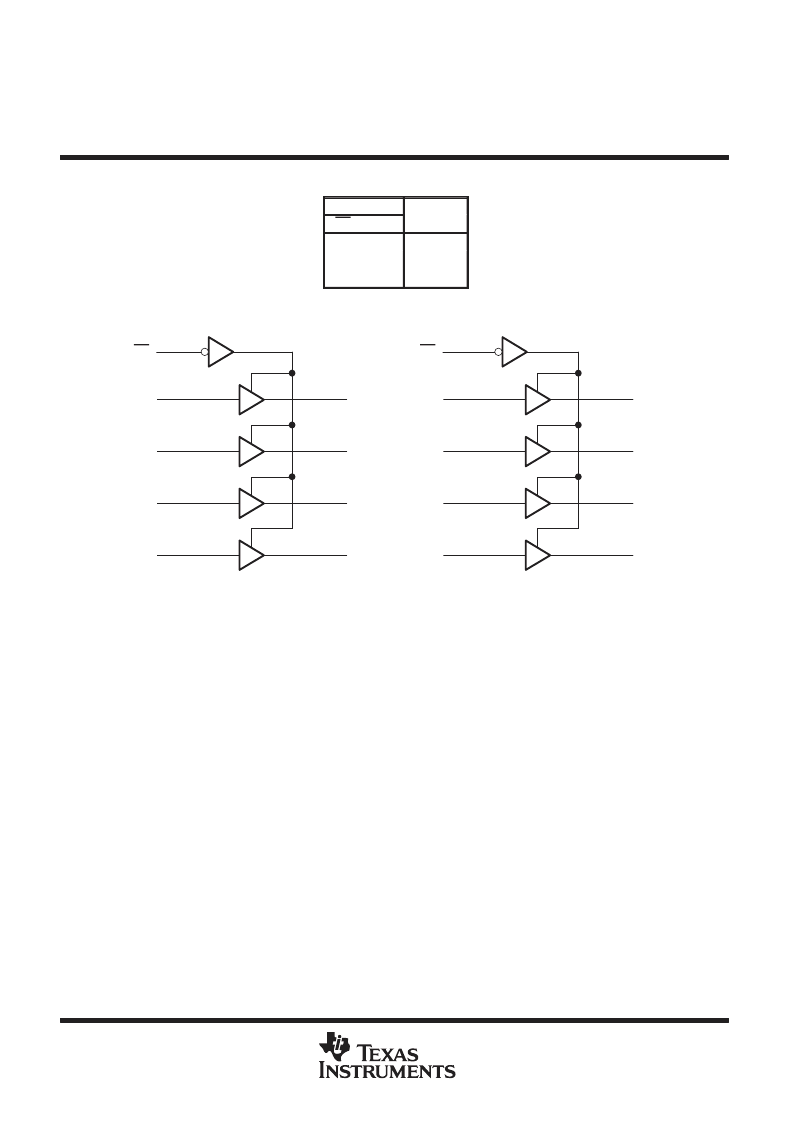
FUNCTION TABLE
(each buffer)
INPUTS
OE
OUTPUT
Y
A
L
H
H
L
L
L
H
X
Z
logic diagram (positive logic)
1
2
18
1Y1
1OE
1A1
4
16
1Y2
1A2
6
14
1Y3
1A3
8
12
1Y4
1A4
19
11
9
2Y1
2OE
2A1
13
7
2Y2
2A2
15
5
2Y3
2A3
17
3
2Y4
2A4
absolute maximum ratings over operating free-air temperature range (unless otherwise noted)
Supply voltage range, V
CC
Input voltage range, V
I
(see Note 1)
Voltage range applied to any output in the high-impedance or power-off state, V
O
(see Note 1)
. . . . . . . . . . . . . . . . . . . . . . . . . . . . . . . . . . . . . . . . . . . . . . . . . . . . . . . . . . . . . . . . . . .
Voltage range applied to any output in the high or low state, V
O
(see Notes 1 and 2)
. . . . . . . . . . . . . . . . . . . . . . . . . . . . . . . . . . . . . . . . . . . . . . . . . . . . . . .
Input clamp current, I
IK
(V
I
< 0 )
. . . . . . . . . . . . . . . . . . . . . . . . . . . . . . . . . . . . . . . . . . . . . . . . . . . . . . . . . .
Output clamp current, I
OK
(V
O
< 0)
. . . . . . . . . . . . . . . . . . . . . . . . . . . . . . . . . . . . . . . . . . . . . . . . . . . . . . . .
Continuous output current, I
O
. . . . . . . . . . . . . . . . . . . . . . . . . . . . . . . . . . . . . . . . . . . . . . . . . . . . . . . . . . . . .
Continuous current through V
CC
or GND
. . . . . . . . . . . . . . . . . . . . . . . . . . . . . . . . . . . . . . . . . . . . . . . . . .
Package thermal impedance,
θ
JA
(see Note 3): DB package
DW package
N package
NS package
PW package
Storage temperature range, T
stg
. . . . . . . . . . . . . . . . . . . . . . . . . . . . . . . . . . . . . . . . . . . . . . . . . . .
Stresses beyond those listed under “absolute maximum ratings” may cause permanent damage to the device. These are stress ratings only, and
functional operation of the device at these or any other conditions beyond those indicated under “recommended operating conditions” is not
implied. Exposure to absolute-maximum-rated conditions for extended periods may affect device reliability.
NOTES:
1. The input negative-voltage and output voltage ratings may be exceeded if the input and output current ratings are observed.
2. The value of VCC is provided in the recommended operating conditions table.
3. The package thermal impedance is calculated in accordance with JESD 51-7.
–0.5 V to 6.5 V
–0.5 V to 6.5 V
. . . . . . . . . . . . . . . . . . . . . . . . . . . . . . . . . . . . . . . . . . . . . . . . . . . . . . . . .
. . . . . . . . . . . . . . . . . . . . . . . . . . . . . . . . . . . . . . . . . . . . . . . . .
–0.5 V to 6.5 V
–0.5 V to V
CC
+ 0.5 V
–50 mA
–50 mA
±
50 mA
±
100 mA
70
°
C/W
58
°
C/W
69
°
C/W
60
°
C/W
83
°
C/W
. . . . . . . . . . . . . . . . . . . . . . . . . . . . . . . . .
. . . . . . . . . . . . . . . . . . . . . . . . . . . . . . . . .
. . . . . . . . . . . . . . . . . . . . . . . . . . . . . . . . . . .
. . . . . . . . . . . . . . . . . . . . . . . . . . . . . . . . .
. . . . . . . . . . . . . . . . . . . . . . . . . . . . . . . . .
–65
°
C to 150
°
C
相关PDF资料 |
PDF描述 |
|---|---|
| SN74LVCZ244ANE4 | OCTAL BUFFER/DRIVER WITH 3-STATE OUTPUTS |
| SN74LVCZ244ADWE4 | OCTAL BUFFER/DRIVER WITH 3-STATE OUTPUTS |
| SN74LVCZ244ADWG4 | OCTAL BUFFER/DRIVER WITH 3-STATE OUTPUTS |
| SN74LVT16244BGRDR | 3.3-V ABT 16-BIT BUFFERS/DRIVERS WITH 3-STATE OUTPUTS |
| SNJ54LVT16244BWD | 3.3-V ABT 16-BIT BUFFERS/DRIVERS WITH 3-STATE OUTPUTS |
相关代理商/技术参数 |
参数描述 |
|---|---|
| SN74LVCZ244ANE4 | 功能描述:缓冲器和线路驱动器 Octal Buffer/Driver W/3-State Output RoHS:否 制造商:Micrel 输入线路数量:1 输出线路数量:2 极性:Non-Inverting 电源电压-最大:+/- 5.5 V 电源电压-最小:+/- 2.37 V 最大工作温度:+ 85 C 安装风格:SMD/SMT 封装 / 箱体:MSOP-8 封装:Reel |
| SN74LVCZ244ANS | 制造商:Texas Instruments 功能描述:IC,Logic,LVC Series |
| SN74LVCZ244ANSR | 功能描述:缓冲器和线路驱动器 Octal Buffer/Driver W/3-State Output RoHS:否 制造商:Micrel 输入线路数量:1 输出线路数量:2 极性:Non-Inverting 电源电压-最大:+/- 5.5 V 电源电压-最小:+/- 2.37 V 最大工作温度:+ 85 C 安装风格:SMD/SMT 封装 / 箱体:MSOP-8 封装:Reel |
| SN74LVCZ244ANSRE4 | 功能描述:缓冲器和线路驱动器 24-Bit FET 2.5/3.3-V Lo-Vltg Bus Switch RoHS:否 制造商:Micrel 输入线路数量:1 输出线路数量:2 极性:Non-Inverting 电源电压-最大:+/- 5.5 V 电源电压-最小:+/- 2.37 V 最大工作温度:+ 85 C 安装风格:SMD/SMT 封装 / 箱体:MSOP-8 封装:Reel |
| SN74LVCZ244ANSRG4 | 功能描述:缓冲器和线路驱动器 Octal Buffer Driver RoHS:否 制造商:Micrel 输入线路数量:1 输出线路数量:2 极性:Non-Inverting 电源电压-最大:+/- 5.5 V 电源电压-最小:+/- 2.37 V 最大工作温度:+ 85 C 安装风格:SMD/SMT 封装 / 箱体:MSOP-8 封装:Reel |
发布紧急采购,3分钟左右您将得到回复。