- 您现在的位置:买卖IC网 > PDF目录98127 > SN74LVT652PWR (TEXAS INSTRUMENTS INC) LVT SERIES, 8-BIT REGISTERED TRANSCEIVER, TRUE OUTPUT, PDSO24 PDF资料下载
参数资料
| 型号: | SN74LVT652PWR |
| 厂商: | TEXAS INSTRUMENTS INC |
| 元件分类: | 总线收发器 |
| 英文描述: | LVT SERIES, 8-BIT REGISTERED TRANSCEIVER, TRUE OUTPUT, PDSO24 |
| 封装: | PLASTIC, TSSOP-24 |
| 文件页数: | 1/11页 |
| 文件大小: | 179K |
| 代理商: | SN74LVT652PWR |
SN54LVT652, SN74LVT652
3.3-V ABT OCTAL BUS TRANSCEIVERS AND REGISTERS
WITH 3-STATE OUTPUTS
SCBS141E – MAY 1992 – REVISED JULY 1995
1
POST OFFICE BOX 655303
DALLAS, TEXAS 75265
D State-of-the-Art Advanced BiCMOS
Technology (ABT) Design for 3.3-V
Operation and Low-Static Power
Dissipation
D Support Mixed-Mode Signal Operation (5-V
Input and Output Voltages With 3.3-V VCC)
D Support Unregulated Battery Operation
Down to 2.7 V
D Typical VOLP (Output Ground Bounce)
< 0.8 V at VCC = 3.3 V, TA = 25°C
D ESD Protection Exceeds 2000 V Per
MIL-STD-883C, Method 3015; Exceeds
200 V Using Machine Model
(C = 200 pF, R = 0)
D Latch-Up Performance Exceeds 500 mA
Per JEDEC Standard JESD-17
D Bus-Hold Data Inputs Eliminate the Need
for External Pullup Resistors
D Support Live Insertion
D Package Options Include Plastic
Small-Outline (DW), Shrink Small-Outline
(DB), and Thin Shrink Small-Outline (PW)
Packages, Ceramic Chip Carriers (FK), and
Ceramic (JT) DIPs
description
These
bus
transceivers
and
registers
are
designed specifically for low-voltage (3.3-V) VCC
operation, but with the capability to provide a TTL
interface to a 5-V system environment.
The ’LVT652 consist of bus transceiver circuits,
D-type flip-flops, and control circuitry arranged for
multiplexed transmission of data directly from the
data bus or from the internal storage registers.
Output-enable (OEAB and OEBA) inputs are provided to control the transceiver functions. Select-control (SAB
and SBA) inputs are provided to select whether real-time or stored data is transferred. The circuitry used for
select control eliminates the typical decoding glitch that occurs in a multiplexer during the transition between
real-time and stored data. A low input selects real-time data and a high input selects stored data. Figure 1
illustrates the four fundamental bus-management functions that can be performed with the
′LVT652.
Copyright
1995, Texas Instruments Incorporated
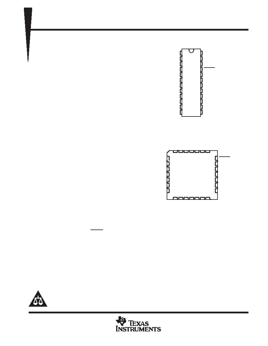
1
2
3
4
5
6
7
8
9
10
11
12
24
23
22
21
20
19
18
17
16
15
14
13
CLKAB
SAB
OEAB
A1
A2
A3
A4
A5
A6
A7
A8
GND
VCC
CLKBA
SBA
OEBA
B1
B2
B3
B4
B5
B6
B7
B8
SN54LVT652 ...JT PACKAGE
SN74LVT652 . . . DB, DW, OR PW PACKAGE
(TOP VIEW)
OEAB
32 1
13 14
5
6
7
8
9
10
11
OEBA
B1
B2
NC
B3
B4
B5
A1
A2
A3
NC
A4
A5
A6
4
15 16 17 18
A8
GND
NC
B8
B7
B6
SAB
CLKAB
NC
SN54LVT652 . . . FK PACKAGE
(TOP VIEW)
28 27 26
25
24
23
22
21
20
19
12
A7
V
CLKBA
SBA
NC – No internal connection
CC
UNLESS OTHERWISE NOTED this document contains PRODUCTION
DATA information current as of publication date. Products conform to
specifications per the terms of Texas Instruments standard warranty.
Production processing does not necessarily include testing of all
parameters.
Please be aware that an important notice concerning availability, standard warranty, and use in critical applications of
Texas Instruments semiconductor products and disclaimers thereto appears at the end of this data sheet.
相关PDF资料 |
PDF描述 |
|---|---|
| SN74LVTH125DG4 | LVT SERIES, QUAD 1-BIT DRIVER, TRUE OUTPUT, PDSO14 |
| SN74LVTH125NSR | LVT SERIES, QUAD 1-BIT DRIVER, TRUE OUTPUT, PDSO14 |
| SN74LVTH126DE4 | LVT SERIES, QUAD 1-BIT DRIVER, TRUE OUTPUT, PDSO14 |
| SN74LVTH126DBR | LVT SERIES, QUAD 1-BIT DRIVER, TRUE OUTPUT, PDSO14 |
| SNJ54LVTH126W | LVT SERIES, QUAD 1-BIT DRIVER, TRUE OUTPUT, CDFP14 |
相关代理商/技术参数 |
参数描述 |
|---|---|
| SN74LVT7244DW | 制造商:Texas Instruments 功能描述: |
| SN74LVT8980ADW | 功能描述:特定功能逻辑 Emb Test-Bus Cntrl w/8-Bit Id Buses RoHS:否 制造商:Texas Instruments 产品: 系列:SN74ABTH18502A 工作电源电压:5 V 封装 / 箱体:LQFP-64 封装:Tube |
| SN74LVT8980ADWR | 功能描述:特定功能逻辑 Emb Test-Bus Cntrl w/8-Bit Id Buses RoHS:否 制造商:Texas Instruments 产品: 系列:SN74ABTH18502A 工作电源电压:5 V 封装 / 箱体:LQFP-64 封装:Tube |
| SN74LVT8980ADWRG4 | 功能描述:特定功能逻辑 Emb Test-Bus Cntrl w/8-Bit Id Buses RoHS:否 制造商:Texas Instruments 产品: 系列:SN74ABTH18502A 工作电源电压:5 V 封装 / 箱体:LQFP-64 封装:Tube |
| SN74LVT8980AIDWREP | 功能描述:特定功能逻辑 Mil Enhance Embedded Test-Bus Cntrlr RoHS:否 制造商:Texas Instruments 产品: 系列:SN74ABTH18502A 工作电源电压:5 V 封装 / 箱体:LQFP-64 封装:Tube |
发布紧急采购,3分钟左右您将得到回复。