- 您现在的位置:买卖IC网 > PDF目录8320 > SN74LVTH574ZQNR (Texas Instruments)IC ABT OCT EDG-TRG D F-F 20-BGA PDF资料下载
参数资料
| 型号: | SN74LVTH574ZQNR |
| 厂商: | Texas Instruments |
| 文件页数: | 12/25页 |
| 文件大小: | 0K |
| 描述: | IC ABT OCT EDG-TRG D F-F 20-BGA |
| 标准包装: | 1,000 |
| 系列: | 74LVTH |
| 功能: | 标准 |
| 类型: | D 型总线 |
| 输出类型: | 三态非反相 |
| 元件数: | 1 |
| 每个元件的位元数: | 8 |
| 频率 - 时钟: | 150MHz |
| 延迟时间 - 传输: | 3ns |
| 触发器类型: | 正边沿 |
| 输出电流高,低: | 32mA,64mA |
| 电源电压: | 2.7 V ~ 3.6 V |
| 工作温度: | -40°C ~ 85°C |
| 安装类型: | 表面贴装 |
| 封装/外壳: | 20-VFBGA |
| 包装: | 带卷 (TR) |
SN54LVTH574, SN74LVTH574
3.3-V ABT OCTAL EDGE-TRIGGERED D-TYPE FLIP-FLOPS
WITH 3-STATE OUTPUTS
SCBS688G MAY 1997 REVISED SEPTEMBER 2003
2
POST OFFICE BOX 655303
DALLAS, TEXAS 75265
description/ordering information (continued)
The eight flip-flops of the ’LVTH574 devices are edge-triggered D-type flip-flops. On the positive transition of
the clock (CLK) input, the Q outputs are set to the logic levels set up at the data (D) inputs.
A buffered output-enable (OE) input can be used to place the eight outputs in either a normal logic state (high
or low logic levels) or a high-impedance state. In the high-impedance state, the outputs neither load nor drive
the bus lines significantly. The high-impedance state and increased drive provide the capability to drive bus
lines without need for interface or pullup components.
OE does not affect the internal operations of the flip-flops. Old data can be retained or new data can be entered
while the outputs are in the high-impedance state.
To ensure the high-impedance state during power up or power down, OE should be tied to VCC through a pullup
resistor; the minimum value of the resistor is determined by the current-sinking capability of the driver.
Active bus-hold circuitry is provided to hold unused or floating data inputs at a valid logic level. Use of pullup
or pulldown resistors with the bus-hold circuitry is not recommended.
These devices are fully specified for hot-insertion applications using Ioff and power-up 3-state. The Ioff circuitry
disables the outputs, preventing damaging current backflow through the devices when they are powered down.
The power-up 3-state circuitry places the outputs in the high-impedance state during power up and power down,
which prevents driver conflict.
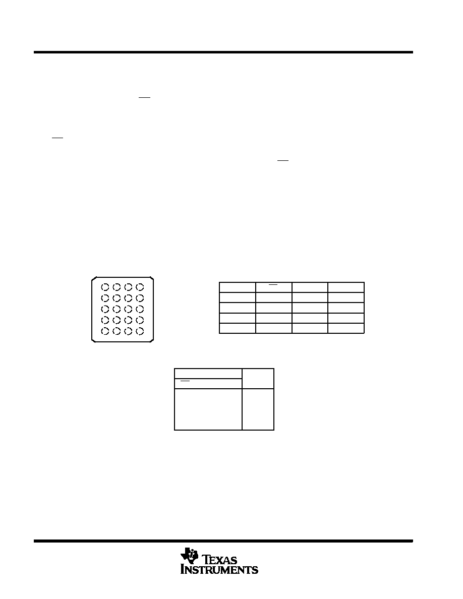
terminal assignments
1234
A
1D
OE
VCC
1Q
B
3D
3Q
2D
2Q
C
5D
4D
5Q
4Q
D
7D
7Q
6D
6Q
E
GND
8D
CLK
8Q
FUNCTION TABLE
(each flip-flop)
INPUTS
OUTPUT
OE
CLK
D
OUTPUT
Q
L
↑
H
L
↑
LL
L
H or L
X
Q0
H
X
Z
SN74LVTH574 . . . GQN OR ZQN PACKAGE
(TOP VIEW)
1
234
A
B
C
D
E
相关PDF资料 |
PDF描述 |
|---|---|
| VI-2WB-MV-F3 | CONVERTER MOD DC/DC 95V 150W |
| RTS-2412/P | CONV DC/DC 2W 24VIN 12VOUT |
| VI-2WB-MV-F2 | CONVERTER MOD DC/DC 95V 150W |
| RTS-2412/H-R | CONV DC/DC 2W 24VIN 12VOUT |
| VI-2WB-MV-F1 | CONVERTER MOD DC/DC 95V 150W |
相关代理商/技术参数 |
参数描述 |
|---|---|
| SN74LVTH62240DGGR | 制造商:Rochester Electronics LLC 功能描述:- Bulk |
| SN74LVTH646DBR | 功能描述:总线收发器 Tri-St ABT Octal Bus RoHS:否 制造商:Fairchild Semiconductor 逻辑类型:CMOS 逻辑系列:74VCX 每芯片的通道数量:16 输入电平:CMOS 输出电平:CMOS 输出类型:3-State 高电平输出电流:- 24 mA 低电平输出电流:24 mA 传播延迟时间:6.2 ns 电源电压-最大:2.7 V, 3.6 V 电源电压-最小:1.65 V, 2.3 V 最大工作温度:+ 85 C 封装 / 箱体:TSSOP-48 封装:Reel |
| SN74LVTH646DBRE4 | 功能描述:总线收发器 3.3V ABT Octal Bus Xcvr/Reg RoHS:否 制造商:Fairchild Semiconductor 逻辑类型:CMOS 逻辑系列:74VCX 每芯片的通道数量:16 输入电平:CMOS 输出电平:CMOS 输出类型:3-State 高电平输出电流:- 24 mA 低电平输出电流:24 mA 传播延迟时间:6.2 ns 电源电压-最大:2.7 V, 3.6 V 电源电压-最小:1.65 V, 2.3 V 最大工作温度:+ 85 C 封装 / 箱体:TSSOP-48 封装:Reel |
| SN74LVTH646DBRG4 | 功能描述:总线收发器 3.3V ABT Octal Bus Transceivr Registr RoHS:否 制造商:Fairchild Semiconductor 逻辑类型:CMOS 逻辑系列:74VCX 每芯片的通道数量:16 输入电平:CMOS 输出电平:CMOS 输出类型:3-State 高电平输出电流:- 24 mA 低电平输出电流:24 mA 传播延迟时间:6.2 ns 电源电压-最大:2.7 V, 3.6 V 电源电压-最小:1.65 V, 2.3 V 最大工作温度:+ 85 C 封装 / 箱体:TSSOP-48 封装:Reel |
| SN74LVTH646DGVR | 功能描述:总线收发器 Tri-St ABT Octal Bus RoHS:否 制造商:Fairchild Semiconductor 逻辑类型:CMOS 逻辑系列:74VCX 每芯片的通道数量:16 输入电平:CMOS 输出电平:CMOS 输出类型:3-State 高电平输出电流:- 24 mA 低电平输出电流:24 mA 传播延迟时间:6.2 ns 电源电压-最大:2.7 V, 3.6 V 电源电压-最小:1.65 V, 2.3 V 最大工作温度:+ 85 C 封装 / 箱体:TSSOP-48 封装:Reel |
发布紧急采购,3分钟左右您将得到回复。