- 您现在的位置:买卖IC网 > PDF目录243974 > SN75240P (TEXAS INSTRUMENTS INC) 60 W, UNIDIRECTIONAL, 2 ELEMENT, SILICON, TVS DIODE, MS-001BA PDF资料下载
参数资料
| 型号: | SN75240P |
| 厂商: | TEXAS INSTRUMENTS INC |
| 元件分类: | 参考电压二极管 |
| 英文描述: | 60 W, UNIDIRECTIONAL, 2 ELEMENT, SILICON, TVS DIODE, MS-001BA |
| 封装: | ROHS COMPLIANT, PLASTIC, MS-001, DIP-8 |
| 文件页数: | 1/14页 |
| 文件大小: | 678K |
| 代理商: | SN75240P |
SN65220
SN65240
SN75240
SLLS266G FEBRUARY 1997 REVISED JULY AUGUST 2008
USB PORT TRANSIENT SUPPRESSORS
YZB-4
DBV-6
PW-8
P-8
FEATURES
D Design to Protect Submicron 3-V or 5-V
Circuits from Noise Transients
D Port ESD Protection Capability Exceeds:
15-kV Human Body Model
2-kV Machine Model
D Available in a WCSP Chip-Scale Package
D Stand-Off Voltage ... 6 V Min
D Low Current Leakage ... 1 A Max at 6 V
D Low Capacitance ... 35 pF Typical
DESCRIPTION
The SN65220 is a single transient voltage suppressor and
the SN65240 and SN75240 are dual transient voltage
suppressors designed to provide electrical noise transient
protection to Universal Serial Bus (USB) fullspeed ports.
Note that the input capacitance of the device makes it
unsuitable for high-speed USB 2.0 applications.
Any cabled I/O can be subjected to electrical noise
transients from various sources. These noise transients
can cause damage to the USB transceiver and/or the USB
ASIC if they are of sufficient magnitude and duration.
USB ports are typically implemented in 3-V or 5-V digital
CMOS with very limited ESD protection. The SN65220,
SN65240, and SN75240 can significantly increase the
port ESD protection level and reduce the risk of damage
to the circuits of the USB port.
The IEC1000-4-2 ESD performance of the SN65220,
SN65240, and SN75240 is measured at the system level.
Therefore, system design impacts the results of these
tests. A high compliance level may be attained with proper
board design and layout.
APPLICATIONS
D USB FullSpeed Host, Hub, or Peripheral
Ports
PRODUCTION DATA information is current as of publication date. Products
conform to specifications per the terms of Texas Instruments standard warranty.
Production processing does not necessarily include testing of all parameters.
Please be aware that an important notice concerning availability, standard warranty, and use in critical applications of Texas Instruments
semiconductor products and disclaimers thereto appears at the end of this data sheet.
www.ti.com
Copyright
E 1997 2008, Texas Instruments Incorporated
A1
A2
B2
B1
A
GND
B
SN65220YZB
(Size: 925
mm x 925 mm +6 mm)
(TOP VIEW)
3
2
4
6
(TOP VIEW)
1
NC
GND
NC
A
B
SN65220DBV
GND
5
NC No internal connection
1
2
3
4
8
7
6
5
GND
C
GND
D
A
GND
B
GND
SN65240P, SN65240PW
SN75240P, SN75240PW
(TOP VIEW)
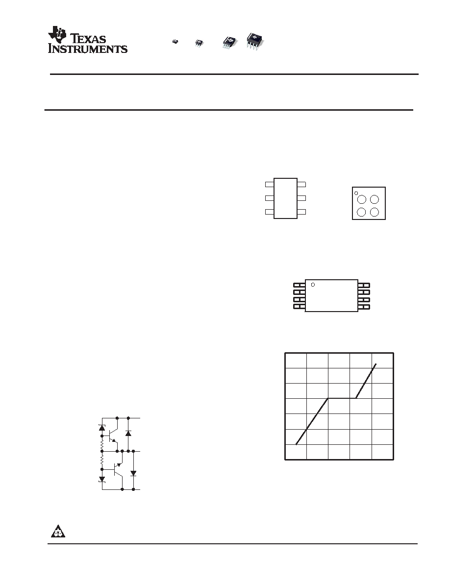
SADI
When read horizontally, Pin 1 is the bottom left pin.
NOTE A:
Typical current versus voltage curve was derived
using the IEC 1.2/50-
s surge waveform.
CURRENT vs VOLTAGE
2.5
5
7.5
10
5
0
2.5
5
10
15
Voltage V
Current
A
10
7.5
A or C
GND
B or D
(One Suppressor Shown)
NOTE: All GND terminals should be connected to ground.
EQUIVALENT SCHEMATIC DIAGRAM
相关PDF资料 |
PDF描述 |
|---|---|
| SFPB-74V | 2 A, SILICON, RECTIFIER DIODE |
| STTA2006PI | 20 A, 600 V, SILICON, RECTIFIER DIODE |
| SMCJ8.5CA-TR | 1500 W, BIDIRECTIONAL, SILICON, TVS DIODE, DO-214AB |
| SQ1216AC | 3.3 pF, SILICON, ABRUPT VARIABLE CAPACITANCE DIODE, DO-7 |
| SQ1728C | VHF-UHF BAND, 15 pF, 30 V, SILICON, ABRUPT VARIABLE CAPACITANCE DIODE, DO-7 |
相关代理商/技术参数 |
参数描述 |
|---|---|
| SN75240P | 制造商:Texas Instruments 功能描述:USB TRANS SUPPRESSOR 75240 DIP8 |
| SN75240P | 制造商:Texas Instruments 功能描述:IC DUAL USB PORT TVS 8-DIP 制造商:Texas Instruments 功能描述:IC, DUAL USB PORT TVS 8-DIP |
| SN75240PE4 | 功能描述:ESD 抑制器 Dual USB Port Transient Suppressor RoHS:否 制造商:STMicroelectronics 通道:8 Channels 击穿电压:8 V 电容:45 pF 端接类型:SMD/SMT 封装 / 箱体:uQFN-16 功率耗散 Pd: 工作温度范围:- 40 C to + 85 C |
| SN75240PW | 功能描述:ESD 抑制器 _ RoHS:否 制造商:STMicroelectronics 通道:8 Channels 击穿电压:8 V 电容:45 pF 端接类型:SMD/SMT 封装 / 箱体:uQFN-16 功率耗散 Pd: 工作温度范围:- 40 C to + 85 C |
| SN75240PWG4 | 功能描述:ESD 抑制器 Dual USB Port Transient Suppressor RoHS:否 制造商:STMicroelectronics 通道:8 Channels 击穿电压:8 V 电容:45 pF 端接类型:SMD/SMT 封装 / 箱体:uQFN-16 功率耗散 Pd: 工作温度范围:- 40 C to + 85 C |
发布紧急采购,3分钟左右您将得到回复。