- 您现在的位置:买卖IC网 > PDF目录225204 > SN75ALS170 (Texas Instruments, Inc.) Triple Differential Bus Transceiver PDF资料下载
参数资料
| 型号: | SN75ALS170 |
| 厂商: | Texas Instruments, Inc. |
| 英文描述: | Triple Differential Bus Transceiver |
| 中文描述: | 三路差动总线收发器 |
| 文件页数: | 13/15页 |
| 文件大小: | 340K |
| 代理商: | SN75ALS170 |
SN75ALS170, SN75ALS170A
TRIPLE DIFFERENTIAL BUS TRANSCEIVER
SLLS055D – AUGUST 1987 – REVISED SEPTEMBER 1995
2–7
POST OFFICE BOX 655303
DALLAS, TEXAS 75265
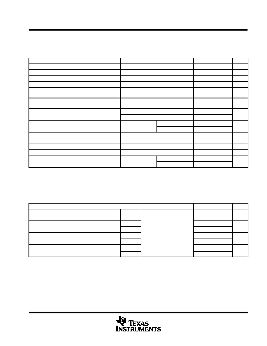
RECEIVER SECTION
electrical characteristics over recommended ranges of common-mode input voltage, supply
voltage, and operating free-air temperature (unless otherwise noted)
PARAMETER
TEST CONDITIONS
MIN
TYP
MAX
UNIT
VIT +
Positive-going input threshold voltage
VO = 2.7 V,
IO = – 0.4 mA
0.3
V
VIT –
Negative-going input threshold voltage
VO = 0.5 V,
IO = 8 mA
– 0.3
V
Vhys
Hysteresis voltage (VIT + – VIT –)
60
mV
VIK
Enable-input clamp voltage
II = – 18 mA
– 1.5
V
VOH
High-level output voltage
VID = 300 mV,
See Figure 5
IOH = – 400 A,
2.7
V
VOL
Low-level output voltage
VID = – 300 mV,
See Figure 5
IOL = 8 mA,
0.45
V
IOZ
High-impedance-state output current
VO = 2.4 V
20
A
IOZ
High-impedance-state output current
VO = 0.4 V
– 400
A
II
Line input current
Other input = 0,
VI = 12 V
1
mA
II
Line input current
Other input
0,
See Note 4
VI = – 7 V
– 0.8
mA
IIH
High-level enable-input current
VIH = 2.7 V
20
A
IIL
Low-level enable-input current
VIL = 0.4 V
– 100
A
rI
Input resistance
12
k
IOS
Short-circuit output current
VID = 300 mV,
VO = 0
–15
–85
mA
ICC
Supply current
No load
Outputs enabled
69
90
mA
ICC
Supply current
No load
Outputs disabled
57
78
mA
All typical values are at VCC = 5 V and TA = 25°C.
The algebraic convention, in which the less-positive (more-negative) limit is designated minimum, is used in this data sheet for common-mode
input voltage and threshold voltage levels only.
NOTE 4: This applies for both power on and off; refer to EIA Standard RS-485 for exact conditions.
switching characteristics over recommended ranges of supply voltage and operating free-air
temperature range
PARAMETER
TEST CONDITIONS
MIN
TYP
MAX
UNIT
tPLH
Propagation delay time, low-to-high-level
ALS170
V
1 5Vt 1 5 V
9
19
ns
tPLH
Propagation delay time, low to high level
output
ALS170A
VID = – 1.5 V to 1.5 V,
CL =15pF
TA =25°C
11.5
16.5
ns
tPHL
Propagation delay time, high-to-low-level
ALS170
CL = 15 pF,
TA = 25°C,
See Figure 6
9
19
ns
tPHL
Propagation delay time, high to low level
output
ALS170A
See Figure 6
11.5
16.5
ns
tsk(p)
Pulse skew§
ALS170
V1 5 V
1 5 V
2
6
ns
tsk(p)
Pulse skew§
ALS170A
VID = – 1.5 V to 1.5 V,
5
ns
tsk(lim)
Skew limit
ALS170
VID
1.5 V to 1.5 V,
CL = 15 pF,
See Figure 6
10
ns
tsk(lim)
Skew limit
ALS170A
5
ns
All typical values are at VCC = 5 V and TA = 25°C.
§ Pulse skew is defined as the | tPLH–tPHL| of each channel.
Skew limit is the maximum difference in propagation delay times between any two channels of one device and between any two devices. This
parameter is applicable at one VCC and operating temperature within the recommended operating conditions.
相关PDF资料 |
PDF描述 |
|---|---|
| SN75ALS172A | Quadruple Differential Line Driver |
| SNA-476-TR1 | 0 MHz - 8000 MHz RF/MICROWAVE WIDE BAND LOW POWER AMPLIFIER |
| SNDR4HX | SLIDE DIP SWITCH-4SWITCHES, SPST, LATCHED,0.025A, 24VDC, THROUGH HOLE-STRAIGHT |
| SNDR6HT | SLIDE DIP SWITCH-6SWITCHES, SPST, LATCHED,0.025A, 24VDC, THROUGH HOLE-STRAIGHT |
| SNJ54LS90J | DECADE, DIVIDE-BY-TWELVE AND BINARY COUNTERS |
相关代理商/技术参数 |
参数描述 |
|---|---|
| SN75ALS170_08 | 制造商:TI 制造商全称:Texas Instruments 功能描述:TRIPLE DIFFERENTIAL BUS TRANSCEIVER |
| SN75ALS170A | 制造商:TI 制造商全称:Texas Instruments 功能描述:TRIPLE DIFFERENTIAL BUS TRANSCEIVER |
| SN75ALS170ADW | 功能描述:SCSI 接口集成电路 Triple Diff Bus RoHS:否 制造商:Texas Instruments 工作电源电压:2.7 V to 5.25 V 电源电流:13 mA 最大工作温度:+ 70 C 最小工作温度:0 C 安装风格:SMD/SMT 封装 / 箱体:SSOP-36 封装:Tube |
| SN75ALS170ADWE4 | 功能描述:SCSI 接口集成电路 Triple Diff Bus Transceiver RoHS:否 制造商:Texas Instruments 工作电源电压:2.7 V to 5.25 V 电源电流:13 mA 最大工作温度:+ 70 C 最小工作温度:0 C 安装风格:SMD/SMT 封装 / 箱体:SSOP-36 封装:Tube |
| SN75ALS170ADWG4 | 功能描述:SCSI 接口集成电路 Triple Differential Bus Transceiver RoHS:否 制造商:Texas Instruments 工作电源电压:2.7 V to 5.25 V 电源电流:13 mA 最大工作温度:+ 70 C 最小工作温度:0 C 安装风格:SMD/SMT 封装 / 箱体:SSOP-36 封装:Tube |
发布紧急采购,3分钟左右您将得到回复。