- 您现在的位置:买卖IC网 > PDF目录374876 > SN8P1703A (SONIX Technology Co., Ltd.) 8-Bit Micro-Controller PDF资料下载
参数资料
| 型号: | SN8P1703A |
| 厂商: | SONIX Technology Co., Ltd. |
| 英文描述: | 8-Bit Micro-Controller |
| 中文描述: | 8位微控制器 |
| 文件页数: | 97/112页 |
| 文件大小: | 634K |
| 代理商: | SN8P1703A |
第1页第2页第3页第4页第5页第6页第7页第8页第9页第10页第11页第12页第13页第14页第15页第16页第17页第18页第19页第20页第21页第22页第23页第24页第25页第26页第27页第28页第29页第30页第31页第32页第33页第34页第35页第36页第37页第38页第39页第40页第41页第42页第43页第44页第45页第46页第47页第48页第49页第50页第51页第52页第53页第54页第55页第56页第57页第58页第59页第60页第61页第62页第63页第64页第65页第66页第67页第68页第69页第70页第71页第72页第73页第74页第75页第76页第77页第78页第79页第80页第81页第82页第83页第84页第85页第86页第87页第88页第89页第90页第91页第92页第93页第94页第95页第96页当前第97页第98页第99页第100页第101页第102页第103页第104页第105页第106页第107页第108页第109页第110页第111页第112页
Preliminary SN8P1702A/SN8P1703A
8-bit micro-controller build-in 12-bit ADC
SONiX TECHNOLOGY CO., LTD
Page 97
Revision 0.5
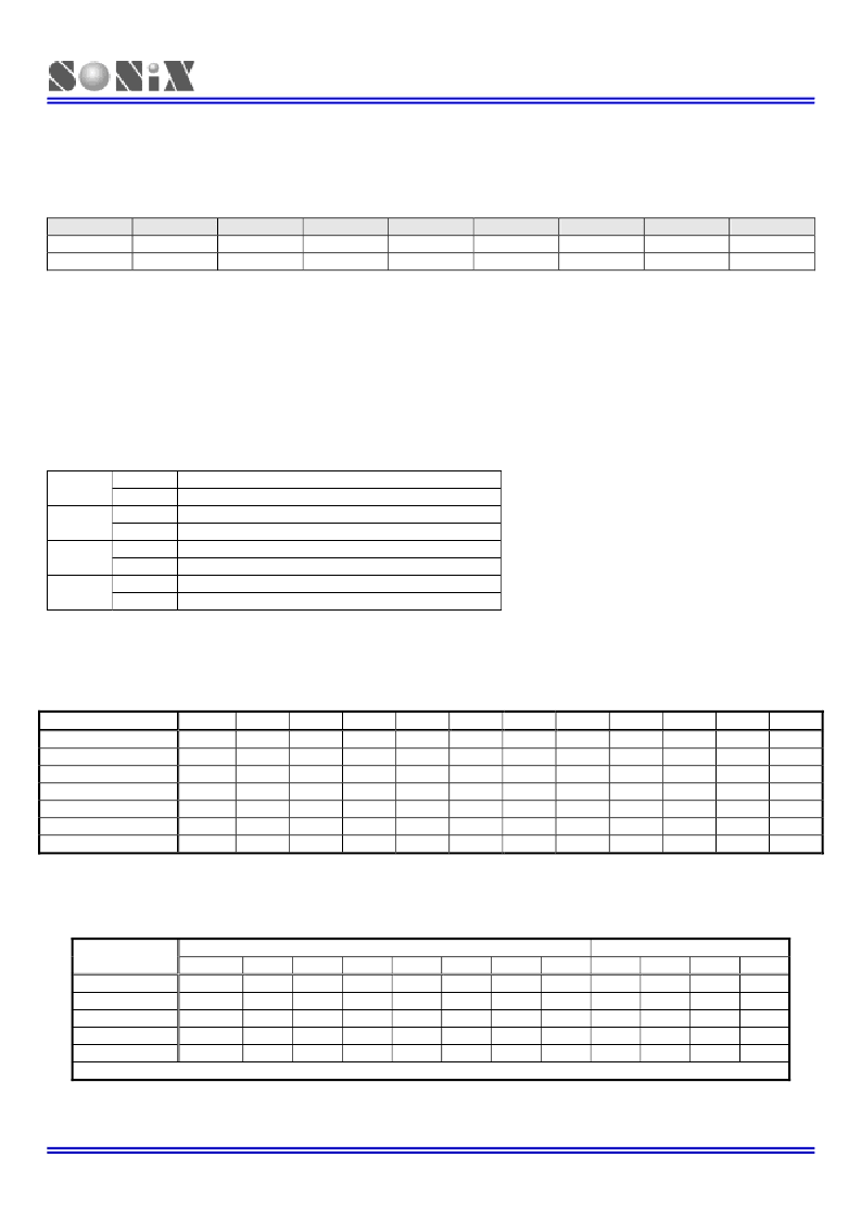
P4CON REGISTERS
ADB initial value = xxxx 0000
0AEH
P4CON
P4CON is Port4 Configuration register. This register can avoid current leakage in unselected ADC channel, which
connected to an analog input source. P4CON [3:0] sets to high will isolate related Port4 digital input path outside chip.
For example, both AIN0 (Port4.0) and AIN1 (Port4.1) are connected to analog input signal, and AIN0 be selected as
conversion channel (CHS [1:0] = 00), this mean the unselected channel P4.1 maybe in digital input mode (if P41M = 0)
In this condition will possible leak current from analog input source. Set P4CON1 = “1” can block P4.1 digital input path
to avoid the current leakage from AIN1.
For the same reason, P4CON0 must set to “1” when conversion channel is AIN1. So any Port4 pin be connected
to analog input source should be set related bit of P4CON as high to avoid unpredictable current leakage. Especially
before entering Sleep mode, remember to set related bit of P4CON as “1”.
Bit [3:0]
P4CON:
Port4 Configuration register.
0
Pass P4.3 digital path into chip.
P4CON3
1
Isolate P4.3 digital path into chip
0
Pass P4.2 digital path into chip.
P4CON2
1
Isolate P4.2 digital path into chip
0
Pass P4.1 digital path into chip.
P4CON1
1
Isolate P4.1 digital path into chip
0
Pass P4.0 digital path into chip.
P4CON0
1
Isolate P4.0 digital path into chip
Note 1: When Port4 is general I/O port, set related P4CON [3:0] = “0”
Note 2: When Port4 is ADC input channel, set related P4CON [3:0] = “1”
The AIN’s input voltage vs. ADB’s output data
AIN n
ADB11 ADB10 ADB9 ADB8
ADB7
0/4096*AVREFH
0
0
0
0
0
1/4096*AVREFH
0
0
0
0
0
.
.
.
.
.
.
.
.
.
.
.
.
.
.
.
.
.
.
4094/4096*AVREFH
1
1
1
1
1
4095/4096*AVREFH
1
1
1
1
1
For different applications, users maybe need more than 8-bit resolution but less than 12-bit ADC converter. To process
the ADB and ADR data can make the job well. First, the AD resolution must be set 12-bit mode and then to execute
ADC converter routine. Then delete the LSB of ADC data and get the new resolution result. The table is as following.
ADB
ADC
Resolution
ADB11
ADB10
ADB9
ADB8
ADB7
8-bit
O
O
O
O
O
9-bit
O
O
O
O
O
10-bit
O
O
O
O
O
11-bit
O
O
O
O
O
12-bit
O
O
O
O
O
O = Selected, x = Delete
Bit 7
0
-
Bit 6
0
-
Bit 5
0
-
Bit 4
0
-
Bit 3
P4CON3
R/W
Bit 2
P4CON2
R/W
Bit 1
P4CON1
R/W
Bit 0
P4CON0
R/W
ADB6
0
0
.
.
.
1
1
ADB5
0
0
.
.
.
1
1
ADB4
0
0
.
.
.
1
1
ADB3 ADB2 ADB1
0
0
0
0
.
.
.
.
.
.
1
1
1
1
ADB0
0
1
.
.
.
0
1
0
0
.
.
.
1
1
ADR
ADB6
O
O
O
O
O
ADB5
O
O
O
O
O
ADB4
O
O
O
O
O
ADB3
x
O
O
O
O
ADB2
x
x
O
O
O
ADB1
x
x
x
O
O
ADB0
x
x
x
x
O
相关PDF资料 |
PDF描述 |
|---|---|
| SN8P1703AP | 8-Bit Micro-Controller |
| SN8P1703AS | 8-Bit Micro-Controller |
| SN8P1703AX | 8-Bit Micro-Controller |
| SN8P1703A-12 | 8-Bit Micro-Controller |
| SN8P1800 | 8-Bit Micro-Controller |
相关代理商/技术参数 |
参数描述 |
|---|---|
| SN8P1703A-12 | 制造商:SONIX 制造商全称:SONIX 功能描述:8-Bit Micro-Controller |
| SN8P1703AP | 制造商:SONIX 制造商全称:SONIX 功能描述:8-Bit Micro-Controller |
| SN8P1703AS | 制造商:SONIX 制造商全称:SONIX 功能描述:8-Bit Micro-Controller |
| SN8P1703AX | 制造商:SONIX 制造商全称:SONIX 功能描述:8-Bit Micro-Controller |
| SN8P1704 | 制造商:SONIX 制造商全称:SONIX 功能描述:8-Bit Micro-Controller |
发布紧急采购,3分钟左右您将得到回复。