- 您现在的位置:买卖IC网 > PDF目录98132 > SNJ54ACT564FK (TEXAS INSTRUMENTS INC) ACT SERIES, 8-BIT DRIVER, INVERTED OUTPUT, CDFP20 PDF资料下载
参数资料
| 型号: | SNJ54ACT564FK |
| 厂商: | TEXAS INSTRUMENTS INC |
| 元件分类: | 总线收发器 |
| 英文描述: | ACT SERIES, 8-BIT DRIVER, INVERTED OUTPUT, CDFP20 |
| 封装: | CERAMIC, DFP-20 |
| 文件页数: | 9/16页 |
| 文件大小: | 584K |
| 代理商: | SNJ54ACT564FK |
SN54ACT564, SN74ACT564
OCTAL D-TYPE EDGE-TRIGGERED FLIP-FLOPS
WITH 3-STATE OUTPUTS
SCAS549B – NOVEMBER 1995 – REVISED NOVEMBER 2002
2
POST OFFICE BOX 655303
DALLAS, TEXAS 75265
description/ordering information (continued)
OE does not affect internal operations of the flip-flops. Old data can be retained or new data can be entered
while the outputs are in the high-impedance state.
To ensure the high-impedance state during power up or power down, OE should be tied to VCC through a pullup
resistor; the minimum value of the resistor is determined by the current-sinking capability of the driver.
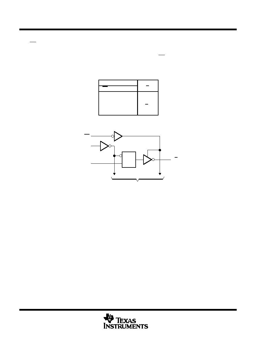
FUNCTION TABLE
(each flip-flop)
INPUTS
OUTPUT
OE
CLK
D
Q
L
↑
H
L
↑
LH
L
H or L
X
Q0
H
X
Z
logic diagram (positive logic)
OE
CLK
1D
1Q
1
11
2
19
To Seven Other Channels
C1
1D
absolute maximum ratings over operating free-air temperature range (unless otherwise noted)
Supply voltage range, VCC
–0.5 V to 7 V
. . . . . . . . . . . . . . . . . . . . . . . . . . . . . . . . . . . . . . . . . . . . . . . . . . . . . . . . . .
Input voltage range, VI (see Note 1)
–0.5 V to VCC + 0.5 V
. . . . . . . . . . . . . . . . . . . . . . . . . . . . . . . . . . . . . . . . . . .
Output voltage range, VO (see Note 1)
–0.5 V to VCC + 0.5 V
. . . . . . . . . . . . . . . . . . . . . . . . . . . . . . . . . . . . . . . .
Input clamp current, IIK (VI < 0 or VI > VCC)
±20 mA
. . . . . . . . . . . . . . . . . . . . . . . . . . . . . . . . . . . . . . . . . . . . . . . .
Output clamp current, IOK (VO < 0 or VO > VCC)
±20 mA
. . . . . . . . . . . . . . . . . . . . . . . . . . . . . . . . . . . . . . . . . . . .
Continuous output current, IO (VO = 0 to VCC)
±50 mA
. . . . . . . . . . . . . . . . . . . . . . . . . . . . . . . . . . . . . . . . . . . . . .
Continuous current through VCC or GND
±200 mA
. . . . . . . . . . . . . . . . . . . . . . . . . . . . . . . . . . . . . . . . . . . . . . . . . .
Package thermal impedance,
θJA (see Note 2): DB package
70
°C/W
. . . . . . . . . . . . . . . . . . . . . . . . . . . . . . . . .
DW package
58
°C/W
. . . . . . . . . . . . . . . . . . . . . . . . . . . . . . . . .
N package
69
°C/W
. . . . . . . . . . . . . . . . . . . . . . . . . . . . . . . . . . .
NS package
60
°C/W
. . . . . . . . . . . . . . . . . . . . . . . . . . . . . . . . .
PW package
83
°C/W
. . . . . . . . . . . . . . . . . . . . . . . . . . . . . . . . .
Storage temperature range, Tstg
–65
°C to 150°C
. . . . . . . . . . . . . . . . . . . . . . . . . . . . . . . . . . . . . . . . . . . . . . . . . . .
Stresses beyond those listed under “absolute maximum ratings” may cause permanent damage to the device. These are stress ratings only, and
functional operation of the device at these or any other conditions beyond those indicated under “recommended operating conditions” is not
implied. Exposure to absolute-maximum-rated conditions for extended periods may affect device reliability.
NOTES:
1. The input and output voltage ratings may be exceeded if the input and output current ratings are observed.
2. The package thermal impedance is calculated in accordance with JESD 51-7.
相关PDF资料 |
PDF描述 |
|---|---|
| SN74ACT564DWRE4 | ACT SERIES, 8-BIT DRIVER, INVERTED OUTPUT, PDSO20 |
| SNJ54AHC02WR | AHC/VHC/H/U/V SERIES, QUAD 2-INPUT NOR GATE, CDFP14 |
| SN74AHC02DRE4 | AHC/VHC/H/U/V SERIES, QUAD 2-INPUT NOR GATE, PDSO14 |
| SNJ54AHC05W | AHC/VHC/H/U/V SERIES, HEX 1-INPUT INVERT GATE, CDFP14 |
| SN74AHC05DGVRG4 | AHC/VHC/H/U/V SERIES, HEX 1-INPUT INVERT GATE, PDSO14 |
相关代理商/技术参数 |
参数描述 |
|---|---|
| SNJ54ACT564J | 制造商:TI 制造商全称:Texas Instruments 功能描述:OCTAL D-TYPE EDGE-TRIGGERED FLIP-FLOPS WITH 3-STATE OUTPUTS |
| SNJ54ACT564W | 制造商:TI 制造商全称:Texas Instruments 功能描述:OCTAL D-TYPE EDGE-TRIGGERED FLIP-FLOPS WITH 3-STATE OUTPUTS |
| SNJ54ACT573FK | 制造商:TI 制造商全称:Texas Instruments 功能描述:OCTAL D-TYPE TRANSPARENT LATCHES WITH 3-STATE OUTPUTS |
| SNJ54ACT573J | 制造商:TI 制造商全称:Texas Instruments 功能描述:OCTAL D-TYPE TRANSPARENT LATCHES WITH 3-STATE OUTPUTS |
| SNJ54ACT573W | 制造商:Texas Instruments 功能描述:Latch Transparent 3-ST 8-CH D-Type 20-Pin CFPAK Tube |
发布紧急采购,3分钟左右您将得到回复。