- 您现在的位置:买卖IC网 > PDF目录98132 > SNJ54ACT564W (TEXAS INSTRUMENTS INC) ACT SERIES, 8-BIT DRIVER, INVERTED OUTPUT, CDIP20 PDF资料下载
参数资料
| 型号: | SNJ54ACT564W |
| 厂商: | TEXAS INSTRUMENTS INC |
| 元件分类: | 总线收发器 |
| 英文描述: | ACT SERIES, 8-BIT DRIVER, INVERTED OUTPUT, CDIP20 |
| 封装: | CERAMIC, DIP-20 |
| 文件页数: | 1/16页 |
| 文件大小: | 584K |
| 代理商: | SNJ54ACT564W |
SN54ACT564, SN74ACT564
OCTAL D-TYPE EDGE-TRIGGERED FLIP-FLOPS
WITH 3-STATE OUTPUTS
SCAS549B – NOVEMBER 1995 – REVISED NOVEMBER 2002
1
POST OFFICE BOX 655303
DALLAS, TEXAS 75265
D 4.5-V to 5.5-V VCC Operation
D Inputs Accept Voltages to 5.5 V
D Max tpd of 8.5 ns at 5 V
D Inputs Are TTL-Voltage Compatible
D 3-State Inverted Outputs Drive Bus Lines
Directly
D Flow-Through Architecture to Optimize
PCB Layout
D Full Parallel Access for Loading
description/ordering information
The
’ACT564
devices
are
octal
D-type
edge-triggered flip-flops that feature 3-state
outputs designed specifically for driving highly
capacitive or relatively low-impedance loads.
They are particularly suitable for implementing
buffer registers, I/O ports, bidirectional bus
drivers, and working registers.
On the positive transition of the clock (CLK) input,
the Q outputs are set to the complements of the
logic levels set up at the data (D) inputs.
A buffered output-enable (OE) input places the
eight outputs in either a normal logic state (high or
low logic levels) or the high-impedance state. In
the high-impedance state, the outputs neither
load nor drive the bus lines significantly. The
high-impedance
state
and
increased
drive
provide the capability to drive bus lines without
interface or pullup components.
ORDERING INFORMATION
TA
PACKAGE
ORDERABLE
PART NUMBER
TOP-SIDE
MARKING
PDIP – N
Tube
SN74ACT564N
SOIC
DW
Tube
SN74ACT564DW
ACT564
40
°Cto85°C
SOIC – DW
Tape and reel
SN74ACT564DWR
ACT564
–40
°C to 85°C
SOP – NS
Tape and reel
SN74ACT564NSR
ACT564
SSOP – DB
Tape and reel
SN74ACT564DBR
AD564
TSSOP – PW
Tape and reel
SN74ACT564PWR
AD564
CDIP – J
Tube
SNJ54ACT564J
–55
°C to 125°C
CFP – W
Tube
SNJ54ACT564W
LCCC – FK
Tube
SNJ54ACT564FK
Package drawings, standard packing quantities, thermal data, symbolization, and PCB design guidelines are
available at www.ti.com/sc/package.
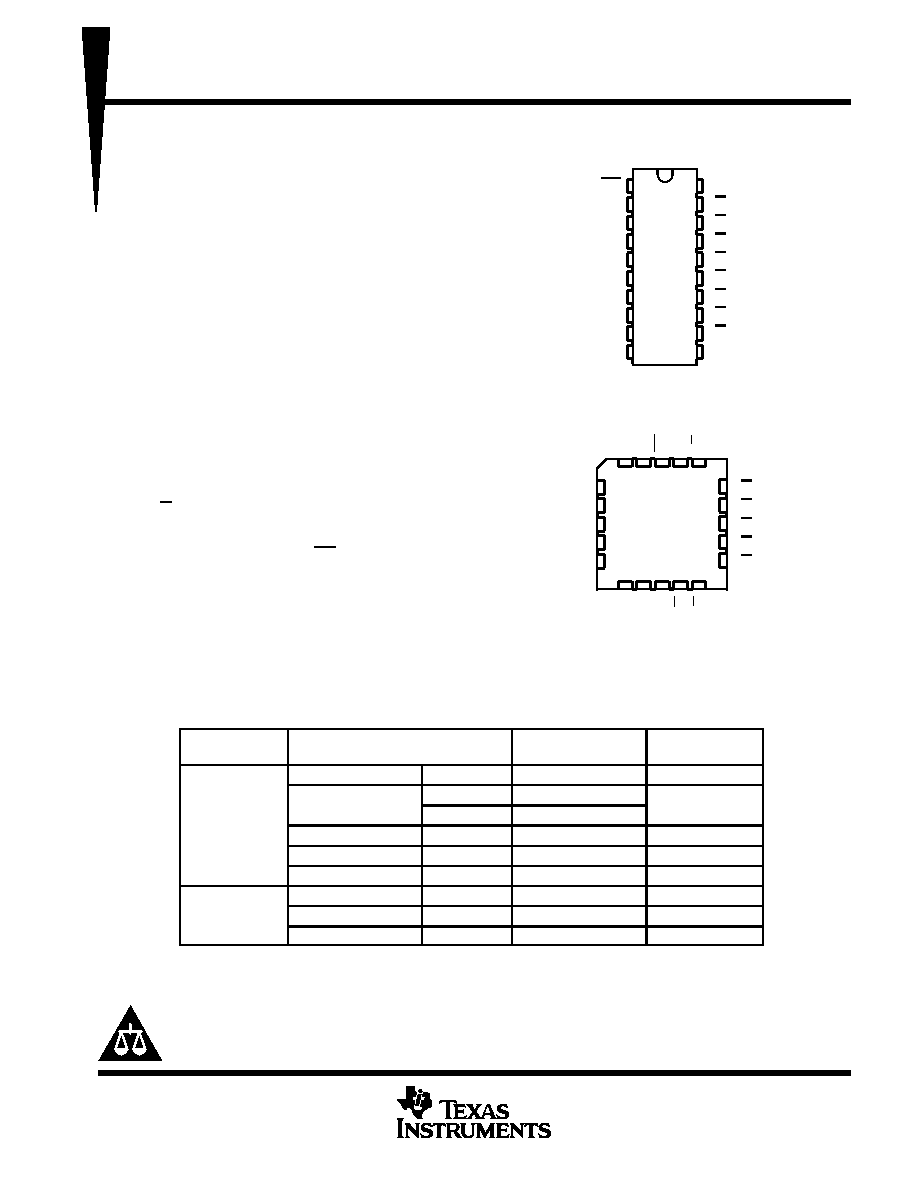
1
2
3
4
5
6
7
8
9
10
20
19
18
17
16
15
14
13
12
11
OE
1D
2D
3D
4D
5D
6D
7D
8D
GND
VCC
1Q
2Q
3Q
4Q
5Q
6Q
7Q
8Q
CLK
SN54ACT564 ...J OR W PACKAGE
SN74ACT564 . . . DB, DW, N, NS, OR PW PACKAGE
(TOP VIEW)
3
2
1 20 19
910 11 12 13
4
5
6
7
8
18
17
16
15
14
2Q
3Q
4Q
5Q
6Q
3D
4D
5D
6D
7D
2D
1D
OE
8Q
7Q
1Q
8D
GND
CLK
V
CC
SN54ACT564 . . . FK PACKAGE
(TOP VIEW)
UNLESS OTHERWISE NOTED this document contains PRODUCTION
DATA information current as of publication date. Products conform to
specifications per the terms of Texas Instruments standard warranty.
Production processing does not necessarily include testing of all
parameters.
Copyright
2002, Texas Instruments Incorporated
Please be aware that an important notice concerning availability, standard warranty, and use in critical applications of
Texas Instruments semiconductor products and disclaimers thereto appears at the end of this data sheet.
相关PDF资料 |
PDF描述 |
|---|---|
| SN74ACT564DBRE4 | ACT SERIES, 8-BIT DRIVER, INVERTED OUTPUT, PDSO20 |
| SNJ54ACT564FK | ACT SERIES, 8-BIT DRIVER, INVERTED OUTPUT, CDFP20 |
| SN74ACT564DWRE4 | ACT SERIES, 8-BIT DRIVER, INVERTED OUTPUT, PDSO20 |
| SNJ54AHC02WR | AHC/VHC/H/U/V SERIES, QUAD 2-INPUT NOR GATE, CDFP14 |
| SN74AHC02DRE4 | AHC/VHC/H/U/V SERIES, QUAD 2-INPUT NOR GATE, PDSO14 |
相关代理商/技术参数 |
参数描述 |
|---|---|
| SNJ54ACT573FK | 制造商:TI 制造商全称:Texas Instruments 功能描述:OCTAL D-TYPE TRANSPARENT LATCHES WITH 3-STATE OUTPUTS |
| SNJ54ACT573J | 制造商:TI 制造商全称:Texas Instruments 功能描述:OCTAL D-TYPE TRANSPARENT LATCHES WITH 3-STATE OUTPUTS |
| SNJ54ACT573W | 制造商:Texas Instruments 功能描述:Latch Transparent 3-ST 8-CH D-Type 20-Pin CFPAK Tube |
| SNJ54ACT574FK | 制造商:TI 制造商全称:Texas Instruments 功能描述:OCTAL D-TYPE EDGE-TRIGGERED FLIP-FLOPS WITH 3-STATE OUTPUTS |
| SNJ54ACT574J | 制造商:TI 制造商全称:Texas Instruments 功能描述:OCTAL D-TYPE EDGE-TRIGGERED FLIP-FLOPS WITH 3-STATE OUTPUTS |
发布紧急采购,3分钟左右您将得到回复。