- 您现在的位置:买卖IC网 > PDF目录98137 > SNJ54HC540W (TEXAS INSTRUMENTS INC) HC/UH SERIES, 8-BIT DRIVER, INVERTED OUTPUT, CDFP20 PDF资料下载
参数资料
| 型号: | SNJ54HC540W |
| 厂商: | TEXAS INSTRUMENTS INC |
| 元件分类: | 总线收发器 |
| 英文描述: | HC/UH SERIES, 8-BIT DRIVER, INVERTED OUTPUT, CDFP20 |
| 封装: | CERAMIC, DFP-20 |
| 文件页数: | 10/17页 |
| 文件大小: | 663K |
| 代理商: | SNJ54HC540W |
SN54HC540, SN74HC540
OCTAL BUFFERS AND LINE DRIVERS
WITH 3STATE OUTPUTS
SCLS007D MARCH 1984 REVISED AUGUST 2003
2
POST OFFICE BOX 655303
DALLAS, TEXAS 75265
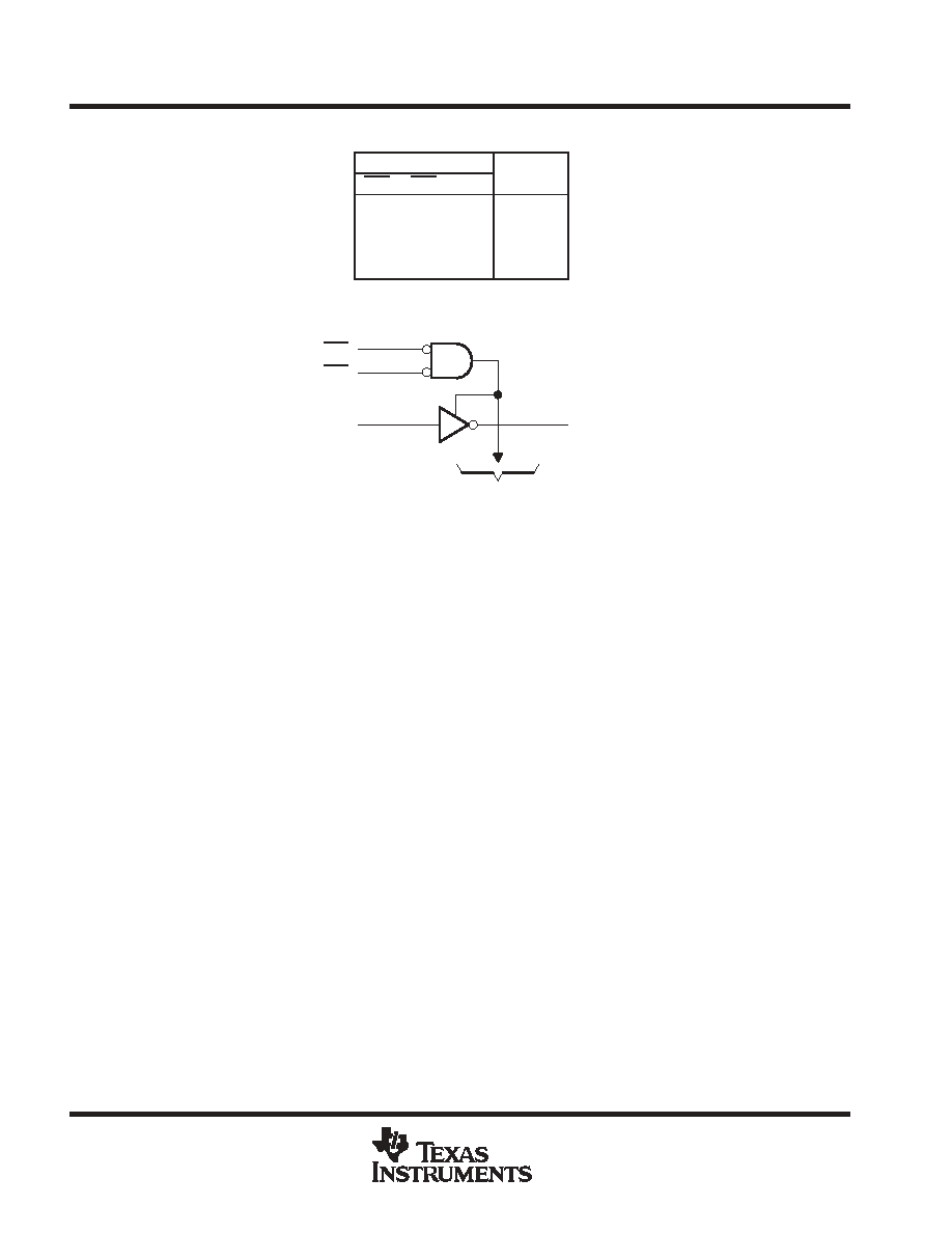
FUNCTION TABLE
(each buffer/driver)
INPUTS
OUTPUT
OE1
OE2
A
OUTPUT
Y
L
H
L
LH
L
H
XX
Z
X
H
X
Z
logic diagram (positive logic)
OE1
OE2
To Seven Other Channels
A1
Y1
1
19
218
absolute maximum ratings over operating free-air temperature range (unless otherwise noted)
Supply voltage range, VCC
0.5 V to 7 V
. . . . . . . . . . . . . . . . . . . . . . . . . . . . . . . . . . . . . . . . . . . . . . . . . . . . . . . . . .
Input clamp current, IIK (VI < 0 or VI > VCC) (see Note 1)
±20 mA
. . . . . . . . . . . . . . . . . . . . . . . . . . . . . . . . . . . .
Output clamp current, IOK (VO < 0 or VO > VCC) (see Note 1)
±20 mA
. . . . . . . . . . . . . . . . . . . . . . . . . . . . . . . .
Continuous output current, IO (VO = 0 to VCC)
±35 mA
. . . . . . . . . . . . . . . . . . . . . . . . . . . . . . . . . . . . . . . . . . . . . .
Continuous current through VCC or GND
±70 mA
. . . . . . . . . . . . . . . . . . . . . . . . . . . . . . . . . . . . . . . . . . . . . . . . . . .
Package thermal impedance,
θJA (see Note 2): DB package
70
°C/W
. . . . . . . . . . . . . . . . . . . . . . . . . . . . . . . . .
DW package
58
°C/W
. . . . . . . . . . . . . . . . . . . . . . . . . . . . . . . . .
N package
69
°C/W
. . . . . . . . . . . . . . . . . . . . . . . . . . . . . . . . . . .
NS package
60
°C/W
. . . . . . . . . . . . . . . . . . . . . . . . . . . . . . . . .
PW package
83
°C/W
. . . . . . . . . . . . . . . . . . . . . . . . . . . . . . . . .
Storage temperature range, Tstg
65
°C to 150°C
. . . . . . . . . . . . . . . . . . . . . . . . . . . . . . . . . . . . . . . . . . . . . . . . . . .
Stresses beyond those listed under “absolute maximum ratings” may cause permanent damage to the device. These are stress ratings only, and
functional operation of the device at these or any other conditions beyond those indicated under “recommended operating conditions” is not
implied. Exposure to absolute-maximum-rated conditions for extended periods may affect device reliability.
NOTES:
1. The input and output voltage ratings may be exceeded if the input and output current ratings are observed.
2. The package thermal impedance is calculated in accordance with JESD 51-7.
相关PDF资料 |
PDF描述 |
|---|---|
| SN74HC540PWT | HC/UH SERIES, 8-BIT DRIVER, INVERTED OUTPUT, PDSO20 |
| SNJ54HC563J | HC/UH SERIES, 8-BIT DRIVER, INVERTED OUTPUT, CDIP20 |
| SNJ54HC563WR | HC/UH SERIES, 8-BIT DRIVER, INVERTED OUTPUT, CDFP20 |
| SNJ54HC563W | HC/UH SERIES, 8-BIT DRIVER, INVERTED OUTPUT, CDFP20 |
| SNJ54HC573AWR | HC/UH SERIES, 8-BIT DRIVER, TRUE OUTPUT, CDFP20 |
相关代理商/技术参数 |
参数描述 |
|---|---|
| SNJ54HC541FK | 制造商:Texas Instruments 功能描述:Buffer/Line Driver 8-CH Non-Inverting 3-ST CMOS 20-Pin LCCC Tube 制造商:Rochester Electronics LLC 功能描述:OCTAL BUFFER/DRIVER - Bulk |
| SNJ54HC541J | 制造商:Texas Instruments 功能描述:OCTAL BUFFER/DRIVER - Rail/Tube |
| SNJ54HC563FK | 制造商:Rochester Electronics LLC 功能描述:- Bulk 制造商:Texas Instruments 功能描述: |
| SNJ54HC573AFK | 制造商:Texas Instruments 功能描述: 制造商:Texas Instruments 功能描述:Latch Transparent 3-ST 8-CH D-Type 20-Pin LCCC Tube |
| SNJ54HC573AJ | 制造商:Texas Instruments 功能描述: 制造商:Texas Instruments 功能描述:Latch Transparent 3-ST 8-CH D-Type 20-Pin CDIP Tube |
发布紧急采购,3分钟左右您将得到回复。