- 您现在的位置:买卖IC网 > PDF目录299918 > SP319CM-L 7 LINE TRANSCEIVER, PQFP80 PDF资料下载
参数资料
| 型号: | SP319CM-L |
| 元件分类: | Buffer和线驱动 |
| 英文描述: | 7 LINE TRANSCEIVER, PQFP80 |
| 封装: | MS-026BEC, LQFP-80 |
| 文件页数: | 15/15页 |
| 文件大小: | 143K |
| 代理商: | SP319CM-L |
9
Rev. 6/10/03
SP319 10Mbps, +5V-Only V.35 Interface with RS-232 (V.28) Control Lines
Copyright 2003 Sipex Corporation
Since both V+ and V- are separately generated
from Vcc in a no load condition, V+and V- will
be symmetrical. Older charge pump approaches
that generate V- from V+ will show a decrease
in the magnitude of V- compared to V+ due to
the inherent inefficiencies in design.
The clock rate for the charge pump typically
operates at 15kHz with 0.1
F, 16V external
capacitors.
Shutdown Mode
The SP319 can be put into a low power
shutdown mode by bringing both TS000 (pin 3)
and ENV35 (pin 9) low. In shutdown mode,
SP319 draws less than 2mA. For normal
operation, both pins should be connected to +5V.
Termination Enable
The SP319 includes a termination enable pin
that connects or disconnects the receiver input
termination circuitry. A TTL logic LOW at ENT
(pin 75) will connect the "Y" termination network
to the V.35 receiver inputs. A TTL logic HIGH
at ENT (pin 75) will disconnect the "Y" termi-
nation network and the receivers will operate as
V.11 compliant receivers. The ENT pin has an
internal pull-down resistor so that a floating
input will enable the termination network. The
SP319 is compatible with the SP320 since pin 75
on the SP320 is designated as a no connect.
External Power Supplies
For applications where separate external
supplies can be applied at the V+ and V- pins.
The value of the external supply voltages should
not exceed +10V. It is critical the external power
supplies provide a power supply sequence of :
+10V, +5V, and then -10V.
Applications Information
The SP319 is a single chip device that can
implement a complete V.35 interface. Three (3)
V.35 drivers and three (3) V.35 receivers are
used for clock and data signals and four (4)
RS-232 (V.28) drivers and four (4) RS-232
(V.28) receivers can be used for the control
signals of the interface. Figures 25 to 28
show the SP319 configured in DTE and DCE
applications along with an ISO-2593 pin out.
+10V
a) C
2
+
GND
b) C
2
–
–10V
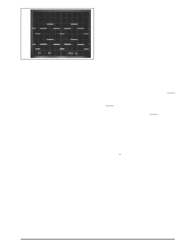
Figure 20. Charge Pump Waveforms
Figure 20 shows the waveforms on the positive
and negative sides of capacitor C2 respectively.
A free-running oscillator controls the four
phases of the voltage shifting. A description
of each phase follows.
Phase 1: V
SS Charge Storage (Figure 21)
During this phase of the clock cycle, the positive
side of capacitors C1 and C2 are charged to
+5V. C1+ is switched to ground and the charge
on C1- is transferred to C2-. Since C2+ is
connected to +5V, the voltage potential across
capacitor C2 becomes 10V.
Phase 2: V
SS Transfer (Figure 22)
Phase two of the clock connects the negative
terminal of C2 to the Vss storage capacitor
and the positive terminal of C2 to ground,
and transfers the generated -10V to C3.
Simultaneously, the positive side of capacitor
C1 is switched to +5V and the negative side
is connected to ground.
Phase 3: V
DD Charge Storage (Figure 23)
The third phase of the clock is identical to
the first phase - the transferred charge on C1
produces -5V on the negative terminal of C1,
which is applied to the negative side of
capacitor C2. Since C2+ is at +5V, the voltage
potential across C2 is +10V.
Phase 4: V
DD Transfer (Figure 24)
The fourth phase of the clock connects the
negative terminal of C2 to ground and transfers
the generated +10V across C2 to C4, the Vdd
storage capacitor. The positive side of capacitor
C1 is switched to +5V and the negative side is
connected to ground, and the cycle begins again.
相关PDF资料 |
PDF描述 |
|---|---|
| SP5769/KG/MP1T | PLL FREQUENCY SYNTHESIZER, 3000 MHz, PDSO16 |
| SP6659EK1-1.5/TR | 1.3 A SWITCHING REGULATOR, 1800 kHz SWITCHING FREQ-MAX, PDSO5 |
| SP7800ABN | 1-CH 12-BIT SUCCESSIVE APPROXIMATION ADC, PARALLEL ACCESS, PDIP24 |
| SP7800AAS | 1-CH 12-BIT SUCCESSIVE APPROXIMATION ADC, PARALLEL ACCESS, PDSO24 |
| SP7800ABS | 1-CH 12-BIT SUCCESSIVE APPROXIMATION ADC, PARALLEL ACCESS, PDSO24 |
相关代理商/技术参数 |
参数描述 |
|---|---|
| SP31R0JT | 功能描述:电流传感电阻器 - SMD SP3 1R0 5% TAPED RoHS:否 制造商:Vishay/Dale 电阻:10 mOhms 功率额定值:1 W 容差:1 % 外壳代码 - in:2512 外壳代码 - mm:6432 温度系数:75 PPM / C 系列:WSL 工作温度范围:- 65 C to + 170 C 产品:Power Metal Strip Resistors Low Value |
| SP32 | 制造商:VOLT PLASTICS 功能描述: |
| SP-32 | 制造商:Triad Magnetics 功能描述: |
| SP3-2.5-10 | 制造商:RHOMBUS-IND 制造商全称:Rhombus Industries Inc. 功能描述:SP3 Series Mini-SIP Passive Delay Modules |
| SP3-2.5-20 | 制造商:RHOMBUS-IND 制造商全称:Rhombus Industries Inc. 功能描述:SP3 Series Mini-SIP Passive Delay Modules |
发布紧急采购,3分钟左右您将得到回复。