- 您现在的位置:买卖IC网 > PDF目录15362 > SP6123ACN-L (Exar Corporation)IC REG CTRLR BUCK PWM VM 8NSOIC PDF资料下载
参数资料
| 型号: | SP6123ACN-L |
| 厂商: | Exar Corporation |
| 文件页数: | 12/18页 |
| 文件大小: | 0K |
| 描述: | IC REG CTRLR BUCK PWM VM 8NSOIC |
| 标准包装: | 98 |
| PWM 型: | 电压模式 |
| 输出数: | 1 |
| 频率 - 最大: | 550kHz |
| 占空比: | 93% |
| 电源电压: | 3 V ~ 5.5 V |
| 降压: | 是 |
| 升压: | 无 |
| 回扫: | 无 |
| 反相: | 无 |
| 倍增器: | 无 |
| 除法器: | 无 |
| Cuk: | 无 |
| 隔离: | 无 |
| 工作温度: | 0°C ~ 70°C |
| 封装/外壳: | 8-SOIC(0.154",3.90mm 宽) |
| 包装: | 管件 |
�� �
�
�APPLICATIONS� INFORMATION�
�V� GS� .� For� 5V� input,� use� the� R� DS(ON)� specified� at�
�4.5V� V� GS� .� At� the� time� of� this� publication,� ven-�
�dors,� such� as� Fairchild,� Siliconix� and� Interna-�
�tional� Rectifier,� have� started� to� specify� R� DS(ON)�
�at� V� GS� less� than� 3V.� This� data� is� necessary� for�
�designs� where� the� MOSFETs� are� driven� with�
�3.3V.�
�Thermal� calculation� must� be� conducted� to� en-�
�sure� the� MOSFET� can� handle� the� maximum�
�load� current.� The� junction� temperature� of� the�
�MOSFET,� determined� as� follows,� must� stay�
�below� the� maximum� rating.�
�forward� voltage.� The� reverse� voltage� across� the�
�diode� is� equal� to� input� voltage,� and� the� diode�
�must� be� able� to� handle� the� peak� current� equal� to�
�the� maximum� load� current.�
�The� power� dissipation� of� the� Schottky� diode� is�
�determined� by�
�P� DIODE� =� 2V� F� I� OUT� T� NOL� F� S�
�where�
�T� NOL� =� non-overlap� time� between� G� L� and� G� H� .�
�V� F� =� forward� voltage� of� the� Schottky� diode.�
�T� J� (� max)� =� T� A� (max)� +�
�P� MOSFET� (max)�
�R� θ� JA�
�,�
�C2�
�R1�
�COMP�
�SP6123�
�?�
�C1�
�where�
�T� A(max)� =� maximum� ambient� temperature�
�P� MOSFET(max)� =� maximum� power� dissipation� of�
�the� MOSFET�
�R� θ� JA� =� junction� to� ambient� thermal� resistance.�
�R� θ� JA� of� the� device� depends� greatly� on� the� board�
�layout,� as� well� as� device� package.� Significant�
�thermal� improvement� can� be� achieved� in� the� maxi-�
�mum� power� dissipation� through� the� proper� design�
�of� copper� mounting� pads� on� the� circuit� board.� For�
�example,� in� a� SO-8� package,� placing� two� 0.04�
�square� inches� copper� pad� directly� under� the� pack-�
�age,� without� occupying� additional� board� space,�
�can� increase� the� maximum� power� dissipation� from�
�approximately� 1� to� 1.2W.� For� DPAK� package,�
�enlarging� the� tap� mounting� pad� to� 1� square� inches�
�reduces� the� R� θ� JA� from� 96� °� C/W� to� 40� °� C/W.�
�Schottky� Diode� Selection�
�When� paralleled� with� the� bottom� MOSFET,� an�
�optional� Schottky� diode� can� improve� efficiency�
�and� reduce� noise.� Without� this� Schottky� diode,�
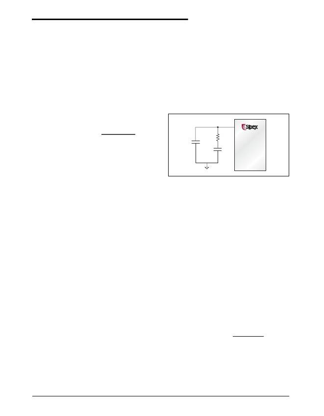
�Figure� 1.� The� RC� network� connected� to� the� COMP� pin�
�provides� a� pole� and� a� zero� to� control� loop.�
�Loop� Compensation� Design�
�The� goal� of� loop� compensation� is� to� manipulate�
�loop� frequency� response� such� that� its� gain� crosses�
�over� 0db� at� a� slope� of� -20db/dec.� The� SP6123�
�has� a� transconductance� error� amplifier� and� re-�
�quires� the� compensation� network� to� be� con-�
�nected� between� the� COMP� pin� and� ground,� as�
�shown� in� Figure� 1.�
�The� first� step� of� compensation� design� is� to� pick�
�the� loop� crossover� frequency.� High� crossover�
�frequency� is� desirable� for� fast� transient� response,�
�but� often� jeopardize� the� system� stability.� Cross-�
�over� frequency� should� be� higher� than� the� ESR�
�zero� but� less� than� 1/5� of� the� switching� fre-�
�quency.� The� ESR� zero� is� contributed� by� the� ESR�
�associated� with� the� output� capacitors� and� can� be�
�determined� by�
�the� body� diode� of� the� bottom� MOSFET� con-�
�ducts� the� current� during� the� non-overlap� time�
�when� both� MOSFETs� are� turned� off.� Unfortu-�
�f� Z(ESR)� =�
�1�
�2� π� C� OUT� R� ESR�
�nately,� the� body� diode� has� high� forward� voltage�
�and� reverse� recovery� problem.� The� reverse� re-�
�covery� of� the� body� diode� causes� additional�
�switching� noises� when� the� diode� turns� off.� The�
�Schottky� diode� alleviates� this� noise� and� addi-�
�tionally� improves� efficiency� thanks� to� its� low�
�Crossover� frequency� of� 20kHz� is� a� sound� first�
�try� if� low� ESR� tantalum� capacitors� or� POSCAPs�
�are� used� at� the� output.� The� next� step� is� to� calcu-�
�late� the� complex� conjugate� poles� contributed� by�
�the� LC� output� filter,�
�Date:� 9/13/04�
�SP6123� Low� Voltage,� Synchronous� Step� Down� PWM� Controller�
�12�
�?� Copyright� 2004� Sipex� Corporation�
�相关PDF资料 |
PDF描述 |
|---|---|
| ECM40DRMN-S288 | CONN EDGECARD 80POS .156 EXTEND |
| IDC7328ER471M | INDUCTOR POWER 470UH 0.82A SMD |
| VE-J1D-EW-F4 | CONVERTER MOD DC/DC 85V 100W |
| ECM40DRMH-S288 | CONN EDGECARD 80POS .156 EXTEND |
| VE-J1D-EW-F2 | CONVERTER MOD DC/DC 85V 100W |
相关代理商/技术参数 |
参数描述 |
|---|---|
| SP6123ACN-L/TR | 功能描述:电压模式 PWM 控制器 Low Voltage, Micro 8 Synchronous, Cntrllr RoHS:否 制造商:Texas Instruments 输出端数量:1 拓扑结构:Buck 输出电压:34 V 输出电流: 开关频率: 工作电源电压:4.5 V to 5.5 V 电源电流:600 uA 最大工作温度:+ 125 C 最小工作温度:- 40 C 封装 / 箱体:WSON-8 封装:Reel |
| SP6123AEN-L | 制造商:Rochester Electronics LLC 功能描述: 制造商:Exar Corporation 功能描述: |
| SP6123CN | 制造商:Exar Corporation 功能描述:Swithed-Mode Power Supply Controller, Voltage Mode Type, 8 Pin, Plastic, SOP |
| SP6123CN/TR | 制造商:SIPEX 制造商全称:Sipex Corporation 功能描述:Low Voltage, Synchronous Step-Down PWM Controller Ideal for 2A to 10A, Small Footprint, DC-DC Power Converters |
| SP6123CN-L | 功能描述:电压模式 PWM 控制器 Low Voltage, Micro 8 Synchronous, Cntrllr RoHS:否 制造商:Texas Instruments 输出端数量:1 拓扑结构:Buck 输出电压:34 V 输出电流: 开关频率: 工作电源电压:4.5 V to 5.5 V 电源电流:600 uA 最大工作温度:+ 125 C 最小工作温度:- 40 C 封装 / 箱体:WSON-8 封装:Reel |
发布紧急采购,3分钟左右您将得到回复。