参数资料
| 型号: | SP6133ER1-L/TR |
| 厂商: | Exar Corporation |
| 文件页数: | 13/20页 |
| 文件大小: | 0K |
| 描述: | IC REG CTRLR BUCK PWM VM 16-QFN |
| 标准包装: | 3,000 |
| PWM 型: | 电压模式 |
| 输出数: | 1 |
| 频率 - 最大: | 345kHz |
| 占空比: | 92% |
| 电源电压: | 5 V ~ 24 V |
| 降压: | 是 |
| 升压: | 无 |
| 回扫: | 无 |
| 反相: | 无 |
| 倍增器: | 无 |
| 除法器: | 无 |
| Cuk: | 无 |
| 隔离: | 无 |
| 工作温度: | -40°C ~ 85°C |
| 封装/外壳: | 16-VFQFN 裸露焊盘 |
| 包装: | 带卷 (TR) |
�� �
�
�APPLICATION� INFORMATION�
�?� Z� (� ESR� )� =�
�?� P(LC)� =�
�ThepowerdissipationoftheSchottkydiode�
�is determined by:�
�P� DIODE� =� 2� ?� V� F� ?� I� OUT� ?� T� NOL� ?� F� S�
�where:�
�T� NOL� =� non-overlap� time� between� GH� and� GL.�
�VF� =� forward� voltage� of� the� Schottky� diode.�
�Loop� Compensation� Design�
�The� open� loop� gain� of� the� whole� system� can�
�be� divided� into� the� gain� of� the� error� ampli-�
�fier, PWM modulator, buck converter output �
�stage,� and� feedback� resistor� divider.� In� or-�
�der to cross over at the selected frequency �
�FCO� , the gain of the error amplifier has to �
�compensate� for� the� attenuation� caused� by�
�the rest of the loop at this frequency.�
�The� goal� of� loop� compensation� is� to� manipu-�
�late loop frequency response such that its �
�gain� crosses� over� 0db� at� a� slope� of� -20db/�
�dec. The first step of compensation design �
�is to pick the loop crossover frequency. High �
�crossover � frequency � is � desirable � for � fast �
�transient� response,� but� often� jeopardizes�
�the � system � stability. � Crossover � frequency �
�should� be� higher� than� the� ESR� zero� but�
�less � than � 1/5 � of � the � switching � frequency. �
�The� ESR� zero� is� contributed� by� the� ESR�
�associated� with� the� output� capacitors� and�
�can be determined by:�
� �
�2� π� ?� C� OUT� ?� R� ESR�
�The� next� step� is� to� calculate� the� complex�
�conjugate� poles� contributed� by� the� LC�
�output filter, �
� �
�2� π� ?� √� L� ?� C� OUT�
�When� the� output� capacitors� are� of� a� Ceramic�
�Type, the SP6133 Evaluation Board requires �
�a� Type� III� compensation� circuit� to� give� a� phase�
�boost of 180° in order to counteract the effects �
�of� an� under� damped� resonance� of� the� output�
�filter at the double pole frequency.�
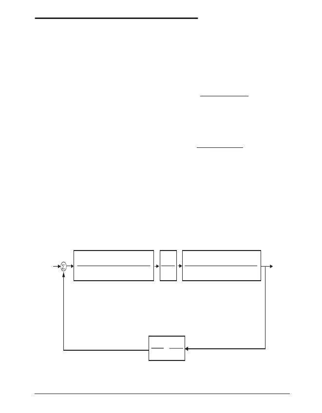
�Type� III� Voltage� Loop�
�Compensation�
�G� AMP� (s)� Gain� Block�
�PWM� Stage�
�G� PWM� Gain�
�Block�
�Output� Stage�
�G� OUT� (s)� Gain�
�Block�
�[S� LC� OUT� +S(R� ESR� +R� DC� )� C� OUT� +1]�
�V� REF�
�(Volts)�
�+�
�_�
�(SRz2Cz2+1)(SR1Cz3+1)�
�SR1Cz2(SRz3Cz3+1)(SRz2Cp1+1)�
�V� IN�
�V� RAMP_PP�
�2�
�(SR� ESR� C� OUT� +� 1)�
�V� OUT�
�(Volts)�
�Notes:� R� ESR� =� Output� Capacitor� Equivalent� Series� Resistance.�
�R� DC� =� Output� Inductor� DC� Resistance.�
�V� RAMP_PP� =� SP6132� Internal� RAMP� Amplitude� Peak� to� Peak� Voltage.�
�Condition:� Cz2� >>� Cp1� &� R1� >>� Rz3�
�Output� Load� Resistance� >>� R� ESR� &� R� DC�
�Voltage� Feedback�
�R� 2� V� REF�
�(R� 1� +� R� 2� )� V� OUT�
�Figure� 5:� SP6133� Voltage�
�Definitions:�
�Mode� Control� Loop� with�
�Loop� Dynamic�
�G� FBK� Gain� Block�
�or�
�V� FBK�
�(Volts)�
�R� ESR� = Output Capacitor Equivalent Series Resistance�
�R� DC� =� Output� Inductor� DC� Resistance�
�V� RAMP� _� PP� =� SP6 33� internal� RAMP� Amplitude� Peak� to� Peak� Voltage�
�Oct� 24-06� Rev� L�
�SP6 33� Synchronous� Buck� Controller�
� 3�
�?� 2006� Sipex� Corporation�
�相关PDF资料 |
PDF描述 |
|---|---|
| SP6134HEU-L | IC REG CTRLR BUCK PWM VM 10-MSOP |
| SP6136ER1-L/TR | IC REG CTRLR BUCK PWM VM 16-QFN |
| SP6137EU-L | IC REG CTRLR BUCK PWM VM 10-MSOP |
| SP6201EM5-G-3-3 | IC REG LDO 3.3V .2A SOT23-5 |
| SP6203EM5-L | IC REG LDO ADJ .3A SOT23-5 |
相关代理商/技术参数 |
参数描述 |
|---|---|
| SP6134 | 制造商:SIPEX 制造商全称:Sipex Corporation 功能描述:Dual Supply Synchronous Buck Controller |
| SP6134_06 | 制造商:SIPEX 制造商全称:Sipex Corporation 功能描述:Dual Supply Synchronous Buck Controller |
| SP61346 | 制造商:SIPEX 制造商全称:Sipex Corporation 功能描述:Dual Supply Synchronous Buck Controller |
| SP6134CU | 制造商:SIPEX 制造商全称:Sipex Corporation 功能描述:Dual Supply Synchronous Buck Controller |
| SP6134CU/TR | 制造商:SIPEX 制造商全称:Sipex Corporation 功能描述:Dual Supply Synchronous Buck Controller |
发布紧急采购,3分钟左右您将得到回复。