- 您现在的位置:买卖IC网 > PDF目录14222 > SP6652ER-L/TR (Exar Corporation)IC REG BUCK SYNC ADJ 1A 10DFN PDF资料下载
参数资料
| 型号: | SP6652ER-L/TR |
| 厂商: | Exar Corporation |
| 文件页数: | 8/16页 |
| 文件大小: | 0K |
| 描述: | IC REG BUCK SYNC ADJ 1A 10DFN |
| 标准包装: | 3,000 |
| 类型: | 降压(降压) |
| 输出类型: | 可调式 |
| 输出数: | 1 |
| 输出电压: | 0.9 V ~ 5 V |
| 输入电压: | 2.85 V ~ 5.5 V |
| PWM 型: | 电流模式 |
| 频率 - 开关: | 1.4MHz |
| 电流 - 输出: | 1A |
| 同步整流器: | 是 |
| 工作温度: | -40°C ~ 85°C |
| 安装类型: | 表面贴装 |
| 封装/外壳: | 10-VFDFN 裸露焊盘 |
| 包装: | 带卷 (TR) |
| 供应商设备封装: | 10-DFN(3x3) |
�� �
�
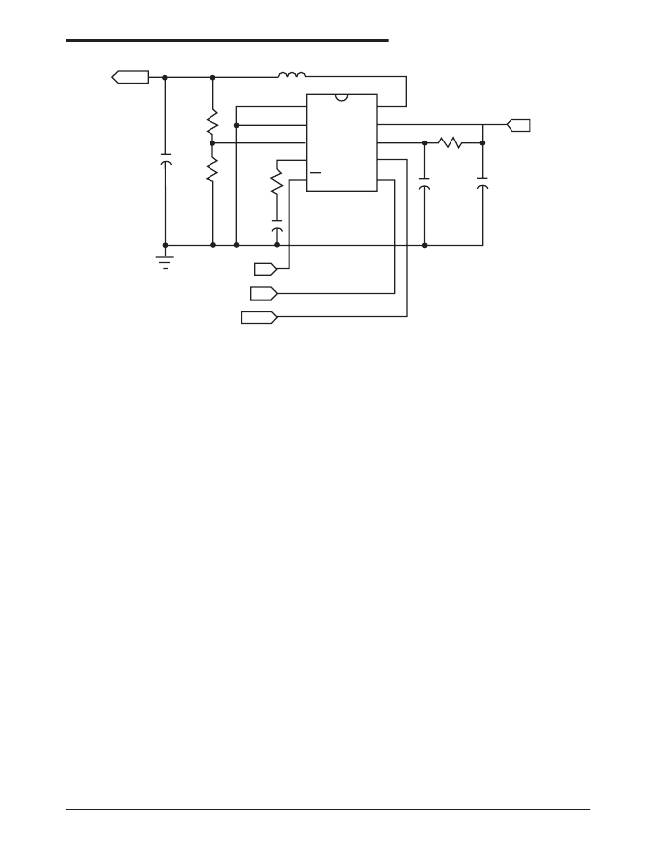
�APPLICATIONS� INFORMATION�
�L1�
�VOUT�
�4.7� μ� H�
�1� PGND�
�LX�
�10�
�R�
�C3�
�10� μ� F�
�FBH�
�R� FBL�
�Rz�
�4k� ?�
�2� SGND�
�3� FB�
�4� COMP�
�5� SD�
�PVIN�
�SVIN�
�SYNC�
�MODE�
�9�
�8�
�7�
�6�
�R1�
�10� ?�
�C2�
�1� μ� F�
�VIN�
�C1�
�10� μ� F�
�SP6652�
�Cc�
�10nF�
�SD�
�V� IN�
�Complete� Application� Circuit.�
�SYNC�
�COMPONENT� SELECTION�
�The� SP6652� PWM� buck� regulator� circuit�
�requires� 3� capacitors:� 10μF� for� the� P� VIN� input,�
�1μF� input� bypass� for� the� S� VIN� and� 10μF�
�for� the� output� are� typically� recommended.�
�For� the� input� capacitor,� a� value� even� larger�
�than� 10μF� will� help� reduce� input� voltage�
�ripple� for� applications� sensitive� to� ripple� on�
�the� battery� voltage.� See� the� Typical� Per� -�
�formance� Characteristics� section� for� wave� -�
�forms� on� input� and� output� ripple� with� 10μF�
�capacitors.� All� the� capacitors� should� be�
�surface� mount� ceramic� for� low� lead� induc� -�
�tance� necessary� at� the� 1.4MHz� switching�
�frequency� of� the� SP6652� and� to� obtain� low�
�ESR.� This� also� helps� improve� bypassing�
�on� the� input� pin� and� ripple� on� the� output.�
�Ceramic� capacitors� with� X5R� or� X7R� tem� -�
�perature� grade� are� recommended� for� most�
�applications.� A� selection� of� recommended�
�capacitors� is� included� in� Table� 1.� The� 1μF�
�S� VIN� input� capacitor� should� have� a� series�
�resistor� of� about� 10Ω� value� connected�
�from� the� input� to� the� S� VIN� pin� to� form� an� RC�
�low� pass� filter� to� remove� high� frequency�
�spikes� present� on� the� input� switching� pin�
�P� VIN� .� This� will� keep� the� SP6652� internal�
�reference� and� other� sensitive� circuits� noise�
�free� and� ensure� better� output� regulation.�
�The� GND� returns� for� the� P� VIN� capacitor� and�
�the� output� capacitor� should� be� connected�
�directly� to� the� P� GND� pin,� which� should� con� -�
�nect� to� the� thermal� pad� ground� located� un� -�
�der� the� SP6652.� The� GND� return� for� the�
�1μF� S� VIN� capacitor� should� be� connected� to�
�the� S� GND� pin,� which� should� be� connected�
�separately� to� the� P� GND� pin� to� avoid� adding�
�P� GND� noise� to� the� SP6652� S� GND� pin.� See�
�the� Typical� SP6652� Circuit� Layout� for� de� -�
�tails� on� the� recommended� layout.�
�Output� Voltage� Selection�
�To� set� the� output� voltage� for� the� SP6652,�
�a� pair� of� resistors,� R� F� and� R� I� are� used� as� a�
�voltage� divider� between� the� output� voltage�
�at� the� output� capacitor� and� the� FB� pin� and�
�GND,� as� shown� in� the� typical� application� cir� -�
�cuit.� The� recommended� value� for� the� R� I� re� -�
�sistor� is� 100K� to� 200K� to� keep� the� quies� -�
�cent� current� low,� but� not� have� the� impedance�
�too� high� at� the� FB� pin� for� good� regulation.�
�Oct10-07� RevJ�
�SP6652� 1A,� High� Efficiency,� Current� Mode� PWM� Buck� Regulator�
�8�
�?� 2007� Sipex� Corporation�
�相关PDF资料 |
PDF描述 |
|---|---|
| MAX6864UK29D1L+T | IC MPU SUPERVISOR SOT23-5 |
| RSM18DTKN-S288 | CONN EDGECARD 36POS .156 EXTEND |
| MAX6864UK30D3L+T | IC MPU SUPERVISOR SOT23-5 |
| RSM18DTKH-S288 | CONN EDGECARD 36POS .156 EXTEND |
| MAX6864UK29D1S+T | IC MPU SUPERVISOR SOT23-5 |
相关代理商/技术参数 |
参数描述 |
|---|---|
| SP6652EU | 制造商:SIPEX 制造商全称:Sipex Corporation 功能描述:Evaluation Board Manual |
| SP6652EU/TR | 制造商:SIPEX 制造商全称:Sipex Corporation 功能描述:1A, High Efficiency, High Frequency Current Mode PWM Buck Regulator |
| SP6652EU-ES | 制造商:SIPEX 制造商全称:Sipex Corporation 功能描述:1A, High Efficiency, Fixed 1.4 MHz Current Mode PWM Buck Regulator |
| SP6652EU-L | 功能描述:开关变换器、稳压器与控制器 High Eff Synchronous Step-Down Converter RoHS:否 制造商:Texas Instruments 输出电压:1.2 V to 10 V 输出电流:300 mA 输出功率: 输入电压:3 V to 17 V 开关频率:1 MHz 工作温度范围: 安装风格:SMD/SMT 封装 / 箱体:WSON-8 封装:Reel |
| SP6652EU-L/TR | 功能描述:开关变换器、稳压器与控制器 High Eff Synchronous Step-Down Converter RoHS:否 制造商:Texas Instruments 输出电压:1.2 V to 10 V 输出电流:300 mA 输出功率: 输入电压:3 V to 17 V 开关频率:1 MHz 工作温度范围: 安装风格:SMD/SMT 封装 / 箱体:WSON-8 封装:Reel |
发布紧急采购,3分钟左右您将得到回复。