- 您现在的位置:买卖IC网 > PDF目录17417 > SP6655EB (Exar Corporation)EVAL BOARD FOR SP6655 PDF资料下载
参数资料
| 型号: | SP6655EB |
| 厂商: | Exar Corporation |
| 文件页数: | 14/17页 |
| 文件大小: | 0K |
| 描述: | EVAL BOARD FOR SP6655 |
| 标准包装: | 1 |
| 系列: | * |
�� �
�
�S� P� 6� 6� 5� 5�
�H� i� g� h� E� f� f� i� c� i� e� n� c� y� 4� 0� 0� m� A� S� y� n� c� h� r� o� n� o� u� s� B� u� c� k� R� e� g� u� l� a� t� o� r�
�supply.� The� typical� input� capacitor� for� the�
�SP6655� is� 10μF� ceramic.� These� capacitors� will�
�provide� good� high� frequency� bypassing� and�
�their� low� ESR� will� reduce� resistive� losses� for�
�higher� efficiency.� An� RC� filter� is� recommended�
�for� the� V� IN� pin� 2� to� effectively� reduce� the� noise�
�for� the� IC's� analog� supply� rail� which� provides�
�power� to� sensitive� circuits.� This� time� constant�
�needs� to� be� at� least� 5� times� greater� than� the�
�switching� period,� which� is� calculated� as� 1/FLP�
�during� the� CCM� mode.� The� typical� application�
�schematic� uses� the� values� of� R� VIN� =� 10Ω� and�
�C� VIN� =� 1� μF� to� meet� these� requirements.�
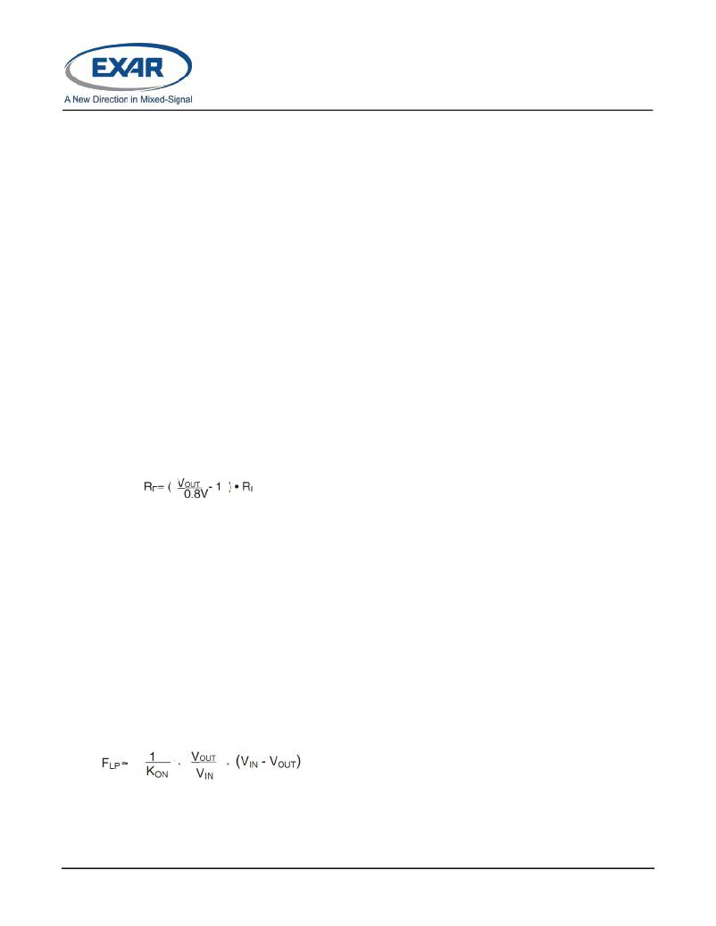
�O� UTPUT� V� OLTAGE� P� ROGRAM�
�The� output� voltage� is� programmed� by� the�
�external� divider,� as� shown� in� the� typical�
�application� circuit� on� page� 1.� First� pick� a� value�
�for� R� I� that� is� no� larger� than� 300KΩ.� Too� large� a�
�value� of� R� I� will� reduce� the� AC� voltage� seen� by�
�the� loop� comparator,� since� the� internal� FB� pin�
�capacitance� can� form� a� low� pass� filter� with� R� F�
�in� parallel� with� R� I� .� The� formula� for� R� F� with� a�
�given� R� I� and� output� voltage� is:�
�O� UTPUT� V� OLTAGE� R� IPPLE� F� REQUENCY�
�An� important� consideration� in� a� power� supply�
�application� is� the� frequency� value� of� the�
�output� ripple.� Given� the� control� technique� of�
�the� SP6655� (as� described� in� the� operations�
�section),� the� frequency� of� the� output� ripple� will�
�vary� when� in� light� to� moderate� load� in� the�
�discontinuous� or� PFM� mode.� For� moderate� to�
�heavy� loads� greater� than� about� 100mA�
�inductor� current� ripple,� (for� the� typical� 10μH�
�inductor� application� on� 100mA� is� half� the�
�200mA� inductor� current� ripple),� the� output�
�ripple� frequency� will� be� fairly� constant.� From�
�the� operations� section,� this� maximum� loop�
�frequency� in� continuous� conduction� mode� is:�
�Data� for� loop� frequency,� as� measured� from�
�output� voltage� ripple� frequency,� can� be� found�
�in� the� typical� performance� curves.�
�L� AYOUT� C� ONSIDERATIONS�
�Proper� layout� of� the� power� and� control� circuits�
�is� necessary� in� a� switching� power� supply� to�
�obtain� good� output� regulation� with� stability�
�and� a� minimum� of� output� noise.� The� SP6655�
�application� circuit� can� be� made� very� small� and�
�reside� close� to� the� IC� for� best� performance�
�and� solution� size,� as� long� as� some� layout�
�techniques� are� taken� into� consideration.� To�
�avoid� excessive� interference� between� the�
�SP6655� high� frequency� converter� and� the�
�other� active� components� on� the� board,� some�
�rules� should� be� followed.� Refer� to� the� typical�
�application� schematic� on� page� 1� and� the�
�sample� PCB� layout� shown� in� the� following�
�figures� to� illustrate� how� to� layout� a� SP6655�
�power� supply.�
�Avoid� injecting� noise� into� the� sensitive� part� of�
�circuit� via� the� ground� plane.� Input� and� output�
�capacitors� conduct� high� frequency� current�
�through� the� ground� plane.� Separate� the�
�control� and� power� grounds� and� connect� them�
�together� at� a� single� point.� Power� ground� plane�
�is� shown� in� the� figure� titled� PCB� top� sample�
�layout� and� connects� the� ground� of� the� C� OUT�
�capacitor� to� the� ground� of� the� C� IN� capacitor�
�and� then� to� the� PGND� pin� 10.� The� control�
�ground� plane� connects� from� pin� 9� GND� to�
�ground� of� the� C� VIN� capacitor� and� the� R� I� ground�
�return� of� the� feedback� resistor.� These� two�
�separate� control� and� power� ground� planes�
�come� together� in� the� figure� titled� PCB� top�
�sample� layout� where� SP6655� pin� 9� GND� is�
�connected� to� pin� 10� PGND.�
�Power� loops� on� the� input� and� output� of� the�
�converter� should� be� laid� out� with� the� shortest�
�and� widest� traces� possible.� The� longer� and�
�narrower� the� trace,� the� higher� the� resistance�
�and� inductance� it� will� have.� The� length� of�
�traces� in� series� with� the� capacitors� increases�
�their� ESR� and� ESL� and� reduces� their�
�effectiveness� at� high� frequencies.� Therefore,�
�put� the� 1μF� bypass� capacitor� as� close� to� the�
�V� IN� and� GND� pins� of� the� converter� as� possible,�
�the� 10μF� C� IN� close� to� the� P� VIN� pin� and� the� 10μF�
�output� capacitor� as� close� to� the� inductor� as�
�possible.� The� external� voltage� feedback�
�network� R� F� ,� R� I� and� feedforward� capacitor� C� F�
�should� be� placed� very� close� to� the� FB� pin.� Any�
�noise� traces� like� the� LX� pin� should� be� kept�
�?� 2012� Exar� Corporation�
�14/17�
�Rev.� 1.0.0�
�相关PDF资料 |
PDF描述 |
|---|---|
| GEM18DSUH | CONN EDGECARD 36POS DIP .156 SLD |
| M7UUK-5005K | IDC CABLE - MDN50K/MC50F/MDN50K |
| F971A476KCC | CAP TANT 47UF 10V 10% SMD |
| EYM06DTMS | CONN EDGECARD 12POS R/A .156 SLD |
| EBM10DCMI | CONN EDGECARD 20POS .156 WW |
相关代理商/技术参数 |
参数描述 |
|---|---|
| SP6655ER | 制造商:Rochester Electronics LLC 功能描述: 制造商:Exar Corporation 功能描述: |
| SP6655ER/TR | 制造商:SIPEX 制造商全称:Sipex Corporation 功能描述:High Efficiency 400mA Synchronous Buck Regulator Ideal for portable designs powered with Li Ion battery |
| SP6655ER-L | 功能描述:DC/DC 开关控制器 Regulator RoHS:否 制造商:Texas Instruments 输入电压:6 V to 100 V 开关频率: 输出电压:1.215 V to 80 V 输出电流:3.5 A 输出端数量:1 最大工作温度:+ 125 C 安装风格: 封装 / 箱体:CPAK |
| SP6655ER-L/TR | 功能描述:DC/DC 开关控制器 High Eff 400mA Synchronous RoHS:否 制造商:Texas Instruments 输入电压:6 V to 100 V 开关频率: 输出电压:1.215 V to 80 V 输出电流:3.5 A 输出端数量:1 最大工作温度:+ 125 C 安装风格: 封装 / 箱体:CPAK |
| SP6655EU-L | 功能描述:开关变换器、稳压器与控制器 High Eff 400mA Synchronous RoHS:否 制造商:Texas Instruments 输出电压:1.2 V to 10 V 输出电流:300 mA 输出功率: 输入电压:3 V to 17 V 开关频率:1 MHz 工作温度范围: 安装风格:SMD/SMT 封装 / 箱体:WSON-8 封装:Reel |
发布紧急采购,3分钟左右您将得到回复。