参数资料
| 型号: | SP723ABG |
| 厂商: | Littelfuse Inc |
| 文件页数: | 2/6页 |
| 文件大小: | 0K |
| 描述: | TVS ARRAY ESD 6 INPUT 8-SOIC |
| 产品培训模块: | Transient Voltage Suppression (TVS) Diodes TVS Diode Array |
| 产品目录绘图: | SP72 Series Circuit |
| 标准包装: | 980 |
| 系列: | SP723 |
| 电压 - 工作: | 30V |
| 技术: | 混合技术 |
| 电路数: | 6 |
| 应用: | 通用 |
| 封装/外壳: | 8-SOIC(0.154",3.90mm 宽) |
| 供应商设备封装: | 8-SOIC |
| 包装: | 管件 |
| 产品目录页面: | 2374 (CN2011-ZH PDF) |
| 其它名称: | F2721 |
�� �
�
�TVS� Diode� Arrays� (SPA� ?� Diodes)�
�General� Purpose� ESD� Protection� -� SP723� Series�
�Absolute� Maximum� Ratings�
�Thermal� Information�
�C/W�
�C/W�
�C�
�Parameter�
�Continuous� Supply� Voltage,� (V+)� -� (V-)�
�Forward� Peak� Current,� I� IN� to� V� CC� ,� I� IN� to�
�GND� (Refer� to� Figure� 5)�
�Peak� Pulse� Current,� 8/20μs�
�Rating�
�+35�
�±4,� 100μs�
�±7�
�Units�
�V�
�A�
�A�
�Parameter�
�Thermal� Resistance� (Typical,� Note� 1)�
�PDIP� Package�
�SOIC� Package�
�Storage� Temperature� Range�
�Rating�
�θ� JA�
�160�
�170�
�-65� to� 150�
�Units�
�o� C/W�
�o�
�o�
�o�
�C�
�C�
�CAUTION:� Stresses� above� those� listed� in� “Absolute� Maximum� Ratings”� may� cause�
�permanent� damage� to� the� device.� This� is� a� stress� only� rating� and� operation� of� the� device�
�at� these� or� any� other� conditions� above� those� indicated� in� the� operational� sections� of� this�
�specification� is� not� implied.�
�Note:�
�Maximum� Junction� Temperature� (Plastic�
�Package)�
�Lead� Temperature�
�(Soldering� 20-40s)� (SOIC� Lead� Tips� Only)�
�150�
�260�
�o�
�o�
�ESD� Ratings� and� Capability� (Figure� 1,� Table� 1)�
�Load� Dump� and� Reverse� Battery� (Note� 2)�
�1.� θ� JA� is� measured� with� the� component� mounted� on� an� evaluation� PC� board� in� free� air.�
�Electrical� Characteristics�
�T� A� =� -40� o� C� to� 105� o� C,� V� IN� =� 0.5V� CC� ,� Unless� Otherwise� Specified�
�Parameter�
�Operating� Voltage� Range,�
�V� SUPPLY� =[(V+)-(V-)]�
�Symbol�
�V� SUPPLY�
�Test� Conditions�
�Min�
�-�
�Typ�
�2� to� 30�
�Max�
�-�
�Units�
�V�
�Forward� Voltage� Drop�
�IN� to� V-�
�V� FWDL�
�I� IN� =2A(Peak� Pulse)�
�-�
�2�
�-�
�V�
�IN� to� V+�
�Input� Leakage� Current�
�Quiescent� Supply� Current�
�Equivalent� SCR� ON� Threshod�
�Equivalent� SCR� ON� Resistance�
�Input� Capacitance�
�Input� Switching� Speed�
�V� FWDH�
�I� IN�
�I� QUIESCENT�
�C� IN�
�t� ON�
�Note� 3�
�V� FWD� /I� FWD� ;� Note� 3�
�-�
�-20�
�-�
�-�
�-�
�-�
�-�
�2�
�5�
�50�
�1.1�
�0.5�
�5�
�2�
�-�
�20�
�200�
�-�
�-�
�-�
�-�
�V�
�nA�
�nA�
�V�
�Ω�
�PF�
�ns�
�Notes:�
�2.� In� automotive� ans� battery� operated� systems,� the� power� supply� lines� should� be� externally� protected� for� load� dump� and� reverse� battery.� When� the� V+� and� V-� Pins� are� connected� to� the� same�
�supply� voltage� source� as� the� device� or� control� line� under� protection,� acurrent� limiting� resistor� should� be� connectied� in� series� between� the� external� supply� and� the� SP723� supply� pins� to�
�limit� reverse� battery� current� to� within� the� rated� maximum� limits.� Bypass� capacitors� of� typically� 0.01μF� or� larger� from� the� V+� and� V-� Pins� to� ground� are� recommended.�
�3.� Refer� to� the� Figure� 3� graph� for� determine� peak� current� and� dessipation� under� EOS� conditions.�
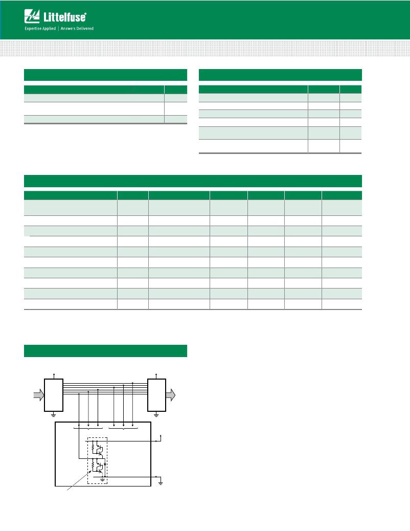
�Typical� Application� of� the� SP723�
�(Application� as� an� Input� Clamp� for� Over-voltage,� Greater� than� 1V� BE�
�Above� V+� or� less� than� -1V� BE� below� V-)�
�+V� CC�
�INPUT�
�DRIVERS�
�OR�
�SIGNAL�
�SOURCES�
�+V� CC�
�LINEAR� OR�
�DIGITAL� IC�
�INTERFACE�
�IN� 1� -� 3�
�IN� 5� -� 7�
�TO� +V� CC�
�V+�
�SP723�
�V-�
�SP723� INPUT� PROTECTION� CIRCUIT� (1� OF� 6� SHO� WN)�
�FIGURE� 4.� TYPICAL� APPLICA� TION� OF� THE� SP723� AS� AN� INPUT� CLAMP� FOR� OVER-VOLTAGE,� GREATER� THAN� 1V� BE� ABOVE� V+� OR�
�LESS� THAN� -1V� BE� BELO� W� V-�
�?� 2013� Littelfuse,� Inc.�
�Specifications� are� subject� to� change� without� notice.�
�Revised:� 04/24/13�
�相关PDF资料 |
PDF描述 |
|---|---|
| MMA25-0341R1 | CONN RACK/PANEL 34POS 5A |
| TL7726ID | IC HEX CLAMPING CIRCUIT 8-SOIC |
| NPTC082KFMS-RC | CONN FEMALE 16POS DL .1" TIN SMD |
| MMA21-0501C1 | CONN RACK/PANEL 50POS 5A |
| CA1-B0-44-610-111-KG | CIRCUIT BREAKER MAGNETIC 10A |
相关代理商/技术参数 |
参数描述 |
|---|---|
| SP723ABG | 制造商:Littelfuse 功能描述:TVS Diode Array |
| SP723ABG | 制造商:Littelfuse 功能描述:THYRISTOR ARRAY TVS |
| SP723ABT | 功能描述:TVS二极管阵列 SP723ABT RoHS:否 制造商:Littelfuse 极性: 通道:4 Channels 击穿电压: 钳位电压:11.5 V 工作电压:2.5 V 峰值浪涌电流:20 A 安装风格:SMD/SMT 端接类型:SMD/SMT 系列: 最小工作温度:- 40 C 最大工作温度:+ 85 C |
| SP723ABTG | 功能描述:TVS二极管阵列 6 CH DIODE ARRAY RoHS:否 制造商:Littelfuse 极性: 通道:4 Channels 击穿电压: 钳位电压:11.5 V 工作电压:2.5 V 峰值浪涌电流:20 A 安装风格:SMD/SMT 端接类型:SMD/SMT 系列: 最小工作温度:- 40 C 最大工作温度:+ 85 C |
| SP723ABTG | 制造商:Littelfuse 功能描述:Diode 制造商:Littelfuse 功能描述:DIODE, TVS, 5pF, SOIC-8 |
发布紧急采购,3分钟左右您将得到回复。