- 您现在的位置:买卖IC网 > PDF目录17413 > SP7650EB (Exar Corporation)EVAL BOARD FOR SP7650 PDF资料下载
参数资料
| 型号: | SP7650EB |
| 厂商: | Exar Corporation |
| 文件页数: | 6/16页 |
| 文件大小: | 0K |
| 描述: | EVAL BOARD FOR SP7650 |
| 标准包装: | 1 |
| 系列: | * |
�� �
�
�THEORY� OF� OPERATION�
�desired,� then� compensation� can� be� as� simple� as�
�an� RC� circuit� to� Ground.� If� a� more� complex�
�compensation� is� required,� then� the� amplifier� has�
�enough� bandwidth� (45� °� at� 4� MHz)� and� enough�
�gain� (60dB)� to� run� Type� III� compensation�
�schemes� with� adequate� gain� and� phase� margins�
�at� crossover� frequencies� greater� than� 50kHz.�
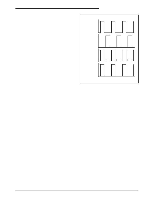
�VBST�
�GH�
�Voltage�
�VSWN�
�V(VCC)�
�GL�
�Voltage�
�The� common� mode� output� of� the� error� amplifier�
�is� 0.9V� to� 2.2V.� Therefore,� the� PWM� voltage�
�ramp� has� been� set� between� 1.1V� and� 2.2V� to�
�ensure� proper� 0%� to� 100%� duty� cycle� capability.�
�The� voltage� loop� also� includes� two� other� very�
�important� features.� One� is� an� asynchronous�
�startup� mode.� Basically,� the� synchronous� recti-�
�fier� cannot� turn� on� unless� the� high� side� switch�
�has� attempted� to� turn� on� or� the� SS� pin� has�
�exceeded� 1.7V.� This� feature� prevents� the� con-�
�troller� from� “dragging� down”� the� output� voltage�
�during� startup� or� in� fault� modes.� The� second�
�feature� is� a� 100%� duty� cycle� timeout� that� en-�
�sures� synchronized� refreshing� of� the� BST� ca-�
�0V�
�V(VIN)�
�SWN�
�Voltage�
�-0V�
�-V(Diode)� V�
�V(VIN)+V(VCC)�
�BST�
�Voltage�
�V(VCC)�
�TIME�
�pacitor� at� very� high� duty� ratios.� In� the� event� that�
�the� high� side� NFET� is� on� for� 20� continuous�
�clock� cycles,� a� reset� is� given� to� the� PWM� flip-�
�flop� half� way� through� the� 21st� cycle.� This� forces�
�GL� to� rise� for� the� cycle,� in� turn� refreshing� the�
�BST� capacitor.� The� boost� capacitor� is� used� to�
�generate� a� high� voltage� drive� supply� for� the� high�
�side� switch,� which� is� 5V� above� V� IN� .�
�Power� MOSFETs�
�The� SP7650� contains� a� pair� of� integrated� low�
�resistance� N-channel� switches� designed� to� drive�
�up� to� 3A� of� output� current.� Care� should� be� taken�
�to� de-rate� the� output� current� based� on� the� ther-�
�mal� conditions� in� the� system� such� as� ambient�
�temperature,� airflow� and� heat� sinking.� Maxi-�
�mum� output� current� could� be� limited� by� thermal�
�limitations� of� a� particular� application� by� taking�
�advantage� of� the� integrated-over-temperature�
�protective� scheme� employed� in� the� SP7650.�
�The� SP7650� incorporates� a� built-in� over-tem-�
�perature� protection� to� prevent� internal� overheat-�
�ing.�
�Setting� Output� Voltages�
�The� SP7650� can� be� set� to� different� output� volt-�
�ages.� The� relationship� in� the� following� formula�
�is� based� on� a� voltage� divider� from� the� output� to�
�the� feedback� pin� VFB,� which� is� set� to� an� internal�
�reference� voltage� of� 0.80V.� Standard� 1%� metal�
�film� resistors� of� surface� mount� size� 0603� are�
�recommended.�
�Vout� =� 0.80V� (� R1� /� R2� +� 1� )� =>�
�R2� =� R1� /� [� (� Vout� /� 0.80V� )� –� 1� ]�
�Where� R1� =� 68.1K� and� for� Vout� =� 0.80V�
�setting,� simply� remove� R2� from� the� board.�
�Furthermore,� one� could� select� the� value� of� the�
�R1� and� R2� combination� to� meet� the� exact�
�output� voltage� setting� by� restricting� R1�
�resistance� range� such� that� 50K� <� R1� <�
�100K� for� overall� system� loop� stability.�
�Date:� 2/16/06�
�SP7650� Wide� Input� Voltage� Range� 3A,� 300kHz,� Buck� Regulator�
�?� Copyright� 2006� Sipex� Corporation�
�Date: / 5/06�
�SP7650� Wide� Input� Voltage� Range� 3A,� 300kHz,� Buck� Regulator�
�6� 6�
�?� Copyright� 2006� Sipex� Corporation�
�相关PDF资料 |
PDF描述 |
|---|---|
| A9BAG-0806F | FLEX CABLE - AFF08G/AF08/AFE08T |
| LM2735SD3.3EVAL | BOARD EVALUATION FOR LM2735 |
| RB-0505D/P | CONV DC/DC 1W 5VIN +/-05VOUT |
| IPS1051LTRPBF | IC IPS SW LOW SIDE 1CH SOT-223 |
| A9CCA-0404E | FLEX CABLE - AFK04A/AE04/AFK04A |
相关代理商/技术参数 |
参数描述 |
|---|---|
| SP7650ER | 制造商:Rochester Electronics LLC 功能描述: 制造商:Exar Corporation 功能描述: |
| SP7650ER/TR | 制造商:SIPEX 制造商全称:Sipex Corporation 功能描述:Wide Input Voltage Range 3A, 300kHz, Buck Regulator |
| SP7650ER-L | 功能描述:直流/直流开关调节器 Buck Regulator RoHS:否 制造商:International Rectifier 最大输入电压:21 V 开关频率:1.5 MHz 输出电压:0.5 V to 0.86 V 输出电流:4 A 输出端数量: 最大工作温度: 安装风格:SMD/SMT 封装 / 箱体:PQFN 4 x 5 |
| SP7650ER-L/TR | 功能描述:直流/直流开关调节器 WIDE INPUT VOLTAGE RANGE, 3A 300k RoHS:否 制造商:International Rectifier 最大输入电压:21 V 开关频率:1.5 MHz 输出电压:0.5 V to 0.86 V 输出电流:4 A 输出端数量: 最大工作温度: 安装风格:SMD/SMT 封装 / 箱体:PQFN 4 x 5 |
| SP7651 | 制造商:SIPEX 制造商全称:Sipex Corporation 功能描述:Evaluation Board Manual |
发布紧急采购,3分钟左右您将得到回复。