- 您现在的位置:买卖IC网 > PDF目录299919 > SPT7855SCN (SIGNAL PROCESSING TECHNOLOGIES) 1-CH 10-BIT SUCCESSIVE APPROXIMATION ADC, PARALLEL ACCESS, PDIP28 PDF资料下载
参数资料
| 型号: | SPT7855SCN |
| 厂商: | SIGNAL PROCESSING TECHNOLOGIES |
| 元件分类: | ADC |
| 英文描述: | 1-CH 10-BIT SUCCESSIVE APPROXIMATION ADC, PARALLEL ACCESS, PDIP28 |
| 封装: | PLASTIC, DIP-28 |
| 文件页数: | 10/11页 |
| 文件大小: | 97K |
| 代理商: | SPT7855SCN |
SPT
8
5/18/98
SPT7855
CLOCK INPUT
The SPT7855 is driven from a single-ended TTL-input clock.
Because the pipelined architecture operates on the rising
edge of the clock input, the device can operate over a wide
range of input clock duty cycles without degrading the dy-
namic performance.
DIGITAL OUTPUTS
The digital outputs (D0-D10) are driven by a separate supply
(OVDD) ranging from +3 V to +5 V. This feature makes it
possible to drive the SPT7855's TTL/CMOS-compatible out-
puts with the user's logic system supply. The format of the
output data (D0-D9) is straight binary. (See table III.) The
outputs are latched on the rising edge of CLK. These outputs
can be switched into a tri-state mode by bringing EN high.
Table III - Output Data Information
ANALOG INPUT
OVERRANGE
OUTPUT CODE
D10
D9-D0
+F.S. + 1/2 LSB
1
11 1111 1111
+F.S. -1/2 LSB
O
11 1111 111
+1/2 F.S.
O
+1/2 LSB
O
OO OOOO OOO
0.0 V
O
OO OOOO OOOO
( indicates the flickering bit between logic 0 and 1.)
OVERRANGE OUTPUT
The OVERRANGE OUTPUT (D10) is an indication that the
analog input signal has exceeded the positive full scale input
voltage by 1 LSB. When this condition occurs, D10 will switch
to logic 1. All other data outputs (D0 to D9) will remain at
logic 1 as long as D10 remains at logic 1. This feature makes
it possible to include the SPT7855 into higher resolution
systems.
EVALUATION BOARD
The EB7855 evaluation board is available to aid designers in
demonstrating the full performance of the SPT7855. This
board includes a reference circuit, clock driver circuit, output
data latches and an on-board reconstruction of the digital
data. An application note describing the operation of this
board as well as information on the testing of the SPT7855 is
also available. Contact the factory for price and availability.
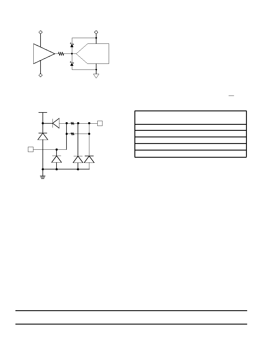
Figure 4 - Recommended Input Protection Circuit
47
D1
D2
ADC
Buffer
AVDD
+V
-V
D1 = D2 = Hewlett Packard HP5712 or equivalent
Figure 5 - On-Chip Protection Circuit
VDD
Analog
Pad
120
120
POWER SUPPLY SEQUENCING CONSIDERATIONS
All logic inputs should be held low until power to the device
has settled to the specific tolerances. Avoid power decou-
pling networks with large time constants which could delay
VDD power to the device.
相关PDF资料 |
PDF描述 |
|---|---|
| SPT7855SCU | 1-CH 10-BIT SUCCESSIVE APPROXIMATION ADC, PARALLEL ACCESS, UUC |
| SPT7860SCS | 1-CH 10-BIT SUCCESSIVE APPROXIMATION ADC, PARALLEL ACCESS, PDSO28 |
| SPT7866SCR | 1-CH 10-BIT PROPRIETARY METHOD ADC, PARALLEL ACCESS, PDSO28 |
| SPT7910SCU | 1-CH 12-BIT FLASH/SUCCESSIVE APPROXIMATION ADC, PARALLEL ACCESS, UUC32 |
| SPT8100SCN | 18-BIT DELTA-SIGMA ADC, SERIAL ACCESS, PDIP32 |
相关代理商/技术参数 |
参数描述 |
|---|---|
| SPT7855SCS | 功能描述:视频模拟/数字化转换器集成电路 10BIT 40MSPS SaR aDC RoHS:否 制造商:Texas Instruments 输入信号类型:Differential 转换器数量:1 ADC 输入端数量:4 转换速率:3 Gbps 分辨率:8 bit 结构: 输入电压:3.3 V 接口类型:SPI 信噪比: 电压参考: 电源电压-最大:3.45 V 电源电压-最小:3.15 V 最大功率耗散: 最大工作温度:+ 85 C 最小工作温度:- 40 C 封装 / 箱体:TCSP-48 封装:Reel |
| SPT7855SCS_Q | 功能描述:模数转换器 - ADC 10BIT 40MSPS SaR aDC RoHS:否 制造商:Texas Instruments 通道数量:2 结构:Sigma-Delta 转换速率:125 SPs to 8 KSPs 分辨率:24 bit 输入类型:Differential 信噪比:107 dB 接口类型:SPI 工作电源电压:1.7 V to 3.6 V, 2.7 V to 5.25 V 最大工作温度:+ 85 C 安装风格:SMD/SMT 封装 / 箱体:VQFN-32 |
| SPT7855SCT | 功能描述:视频模拟/数字化转换器集成电路 10BIT 40MSPS SaR aDC RoHS:否 制造商:Texas Instruments 输入信号类型:Differential 转换器数量:1 ADC 输入端数量:4 转换速率:3 Gbps 分辨率:8 bit 结构: 输入电压:3.3 V 接口类型:SPI 信噪比: 电压参考: 电源电压-最大:3.45 V 电源电压-最小:3.15 V 最大功率耗散: 最大工作温度:+ 85 C 最小工作温度:- 40 C 封装 / 箱体:TCSP-48 封装:Reel |
| SPT7855SCT_Q | 功能描述:模数转换器 - ADC 10BIT 40MSPS SaR aDC RoHS:否 制造商:Texas Instruments 通道数量:2 结构:Sigma-Delta 转换速率:125 SPs to 8 KSPs 分辨率:24 bit 输入类型:Differential 信噪比:107 dB 接口类型:SPI 工作电源电压:1.7 V to 3.6 V, 2.7 V to 5.25 V 最大工作温度:+ 85 C 安装风格:SMD/SMT 封装 / 箱体:VQFN-32 |
| SPT7855SCTX | 功能描述:直流/直流开关转换器 RoHS:否 制造商:STMicroelectronics 最大输入电压:4.5 V 开关频率:1.5 MHz 输出电压:4.6 V 输出电流:250 mA 输出端数量:2 最大工作温度:+ 85 C 安装风格:SMD/SMT |
发布紧急采购,3分钟左右您将得到回复。