- 您现在的位置:买卖IC网 > PDF目录193599 > SPX29150T-2.5 1.5A High Current Low Dropout Voltage Regulator Adjustable & Fixed Output, Fast Response PDF资料下载
参数资料
| 型号: | SPX29150T-2.5 |
| 元件分类: | 线性稳压 |
| 英文描述: | 1.5A High Current Low Dropout Voltage Regulator Adjustable & Fixed Output, Fast Response |
| 中文描述: | 1.5A的高电流低压差稳压器可调节 |
| 文件页数: | 3/9页 |
| 文件大小: | 78K |
| 代理商: | SPX29150T-2.5 |
3
Date:5/25/04
SP29150/51/52/53 1.5A Low Dropout Voltage Regulator
Copyright 2004 Sipex Corporation
at V
IN=VOUT + 1V and IOUT = 10mA, CIN = 6.8F, COUT = 10F, TA = 25°C, unless otherwise specified. The Boldface applies
over the junction temperature range. Adjustable versions are set to 5.0V.
PARAMETER
CONDITIONS
TYP
MIN
MAX
UNITS
FLAG OUTPUT (ERROR COMPARATOR)
SPX29150/29151/29153
Output Leakage
V
OH=16V
0.1
1
A
Current
2
Output Low Voltage
Device set for 5V,V
IN=4.5V, IOL=250A
200
300
mV
400
Upper Threshold
Device set for 5V, (Note 5)
60
40
mV
Voltage
25
Lower Threshold
Device set for 5V, (Note 5)
75
95
mV
Voltage
140
Hysteresis
Device set for 5V, (Note 5)
15
mV
ENABLE Input
SPX29151/29152
Input Logic Voltage
Low (OFF)
V
IN<10V
0.8
V
High (ON)
2.4
ENABLE Input Pin
V
EN=16V
100
600
A
750
V
EN=0.8V
1
A
2
Regulator Output
(Note 6)
10
500
A
Current in Shutdown
Thermal Resistance
TO-200 Junction to Case, at Tab
3
°C/W
TO-220 Junction to Ambient
60
TO-263Junction to Case, at Tab
3
TO-263 Junction to Ambient
60
NOTES:
Note 1: Dropout voltage is defined as the input to output differential when the output voltage drops to 99% of its nominal value.
Note 2: VIN = VOUT (NOMINAL) +1V. For example, use VIN = 4.3V for a 3.3V regulator. Employ pulse-testing procedures to minimize temperature rise.
Note 3: Ground pin current is the regulator quiescent current. The total current drawn from the source is the sum of the load current to the ground current.
Note 4: Thermal regulation is defined as the change in the output voltage at a time T after a change in power dissipation is applied, excluding load or line regulation
effects.
Note 5: Comparator threshold is expressed in terms of a voltage differential at the Adjust terminal below the nominal reference voltage measured 6V input. To
express these thresholds in terms of output voltage change, multiply the error amplifier gain = VOUT/VREF = (R1 + R2)/R2. For example, at a programmable
output voltage of 5V, the Error output is guaranteed to go low when the output drops by 95mVx 5V/ 1.240V = 38mV. Threshold remain constant as a percent of
VOUT as VOUT is varied, with the dropout warning occurring at typically 5% below nominal, 7.7% guaranteed.
Note 6: VEN ≤ 0.8V and VIN ≤ 16V, VOUT = 0.
Note 7: Maximum positive supply voltage of 20V must be of limited duration (<100m_) < 1%. The maximum continuous supply voltage is 16V.
Note 8: VREF≤ VOUT ≤ (VIN-1), 2.5V≤VIN ≤ 16V, 10mA ≤ IL ≤ IFL, Tj < Tjmax.
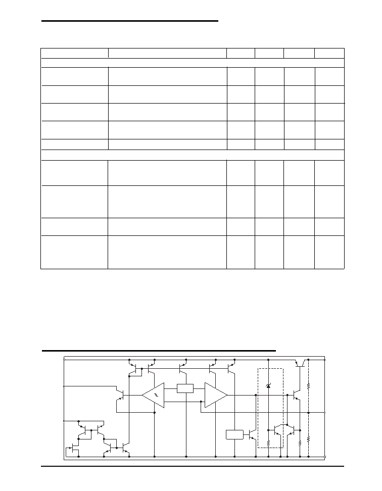
Reference
Thermal
Shutdown
EN
IN
OUT
ADJ
GND
O.V
I
LIMIT
28V
R1*
R2*
1.180V
1.240V
+
--
FLAG
BLOCK DIAGRAM
ELECTRICAL CHARACTERISTICS
相关PDF资料 |
PDF描述 |
|---|---|
| SPX2920M3-5.0 | 400mA Low Drop Out Voltage Regulator with Shutdown |
| SPX2920S | 400mA Low Drop Out Voltage Regulator with Shutdown |
| SPX2920S-2.5 | 400mA Low Drop Out Voltage Regulator with Shutdown |
| SPX2920S-3.3 | 400mA Low Drop Out Voltage Regulator with Shutdown |
| SPX2920S-5.0 | 400mA Low Drop Out Voltage Regulator with Shutdown |
相关代理商/技术参数 |
参数描述 |
|---|---|
| SPX29150T-2-5/TR | 制造商:SIPEX 制造商全称:Sipex Corporation 功能描述:1.5A Low Dropout Voltage Regulator |
| SPX29150T-3.3 | 制造商:SIPEX 制造商全称:Sipex Corporation 功能描述:1.5A Low Dropout Voltage Regulator Adjustable & Fixed Output, Fast Response Time |
| SPX29150T-3.3/TR | 制造商:SIPEX 制造商全称:Sipex Corporation 功能描述:1.5A Low Dropout Voltage Regulator Adjustable & Fixed Output, Fast Response Time |
| SPX29150T-3-3 | 制造商:SIPEX 制造商全称:Sipex Corporation 功能描述:1.5A Low Dropout Voltage Regulator |
| SPX29150T-3-3/TR | 制造商:SIPEX 制造商全称:Sipex Corporation 功能描述:1.5A Low Dropout Voltage Regulator |
发布紧急采购,3分钟左右您将得到回复。