- 您现在的位置:买卖IC网 > PDF目录2165 > SSM2142SZ-REEL (Analog Devices Inc)IC AUDIO DVR MONO AB DIFF 16SOIC PDF资料下载
参数资料
| 型号: | SSM2142SZ-REEL |
| 厂商: | Analog Devices Inc |
| 文件页数: | 5/8页 |
| 文件大小: | 0K |
| 描述: | IC AUDIO DVR MONO AB DIFF 16SOIC |
| 标准包装: | 1,000 |
| 放大器类型: | 音频 |
| 电路数: | 1 |
| 输出类型: | 差分 |
| 转换速率: | 15 V/µs |
| 电流 - 电源: | 5.5mA |
| 电流 - 输出 / 通道: | 70mA |
| 电压 - 电源,单路/双路(±): | ±13 V ~ 18 V |
| 工作温度: | -40°C ~ 85°C |
| 安装类型: | 表面贴装 |
| 封装/外壳: | 16-SOIC(0.295",7.50mm 宽) |
| 供应商设备封装: | 16-SOIC W |
| 包装: | 带卷 (TR) |
SSM2142
–5–
on-chip 50
series damping resistors. The impedances in the
output buffer pair are precisely balanced by laser trimming
during production. This results in the high gain accuracy
needed to obtain good common-mode noise rejection, and
excellent separation between the offset error voltages common
to the cable pair and the desired differential input signal. As
shown in the test circuit, it is suggested that a suitable balanced,
high input-impedance differential amplifier such as the
SSM2141 be used at the receiving end for best system
performance. The SSM2141 receiver output is configured for a
gain of one half following the 6 dB gain of the SSM2142, in
order to maintain an overall system gain of unity.
In applications encountering a large dc offset on the cable or
those wishing to ensure optimal rejection performance by
avoiding differential offset error sources, dc blocking capacitors
may be employed at the sense outputs of the SSM2142. As
shown in the test circuit, these components should present as
little impedance as possible to minimize low-frequency errors,
such as 10
F NP (or tantalum if the polarity of the offset is
known).
SYSTEM GROUNDING CONSIDERATIONS
Due to ground currents, supply variations, and other factors,
the ground potentials of the circuits at each end of a signal cable
may not be exactly equal. The primary purpose of a balanced
pair line is to reject this voltage difference, commonly called
“longitudinal error.” A measure of the ability of the system to
reject longitudinal error voltage is output common-mode
rejection. In order to obtain the optimal OCMR and noise
rejection performance available with the SSM2142, the user
should observe the following precautions:
1. The quality of the differential output is directly dependent
upon the accuracy of the input voltage presented to the
device. Input voltage errors developed across the impedance
of the source must be avoided in order to maintain system
performance. The input of the SSM2142 should be driven
directly by an operational amplifier or buffer offering low
source impedance and low noise.
2. The ground input should be in close proximity to the single-
ended input’s source common. Ground offset errors encoun-
tered in the source circuitry also impair system performance.
3. Make sure that the SSM2142 is adequately decoupled with
0.1
F bypass capacitors located close to each supply pin.
4. Avoid the use of passive circuitry in series with the SSM2142
outputs. Any reactive difference in the line pair will cause
significant imbalances and affect the gain error of the device.
Snubber networks or series load resistors are not required to
maintain stability in SSM2142 based systems, even when
driving signals over extremely long cables.
5. Efforts should be made to maintain a physical balance in the
arrangement of the signal pair wiring. Capacitive differences
due to variations in routing or wire length may cause unequal
noise pickup between the pair, which will degrade the system
OCMR. Shielded twisted-pair cable is the preferred choice in
all applications. The shield should not be utilized as a signal
conductor. Grounding the shield at one end, near the output
common, avoids ground loop currents flowing in the shield
which increase noise coupling and longitudinal errors.
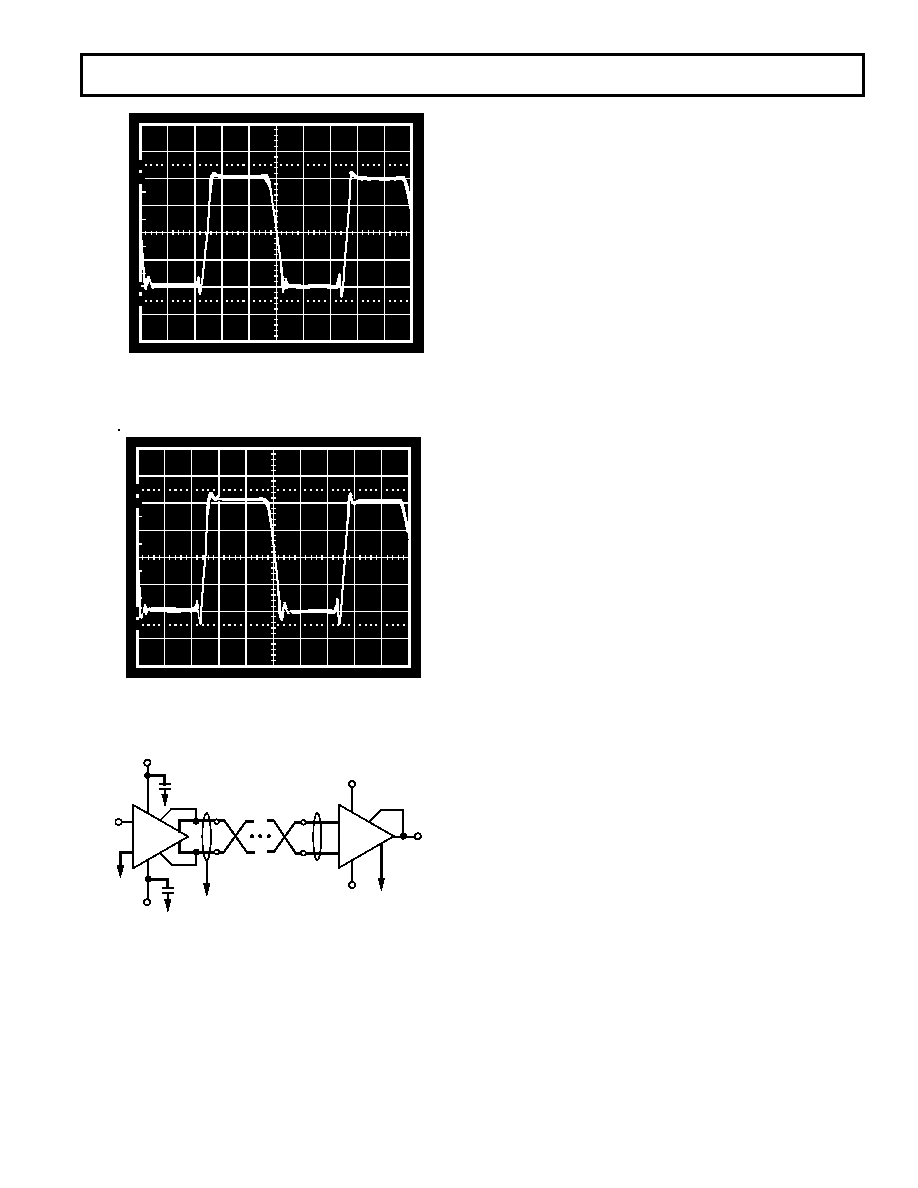
100
90
0%
10
Figure 12. 100 kHz Square Wave Observed at Point B
(Differential Mode). VO = 10 V rms, R1 = R2 = ∞, RL = 600
100
90
0%
10
Figure 13. 100 kHz Square Wave at Point B (Differential
Mode). VO = 10 V rms, R1 = R2 =
∞, R
L = 600
, with
Series Feedback Capacitors
V
IN
SSM
2142
4
3
+15V
6
5
7
8
1
2
–15V
V
OUT
3
2
+15V
7
5
6
1
4
–15V
SHIELDED
TWISTED-PAIR
CABLE
SSM
2141/
2143
Figure 14. Typical Application of the SSM2142 and
SSM2141
APPLICATIONS INFORMATION
The SSM2142 is designed to provide excellent common-mode
rejection, high output drive, and low signal distortion and noise
in a balanced line-driving system. The differential output stage
consists of twin cross-coupled unity gain buffer amplifiers with
REV. C
相关PDF资料 |
PDF描述 |
|---|---|
| SSM2143SZ-REEL | IC AUDIO RX MONO AB DIFF 8SOIC |
| SY84403BLMG TR | IC AMP LIMIT CML 4.25GBPS 10-MLF |
| SY88303BLMG TR | IC AMP CML LIMITING POST 16MLF |
| SY88305BLMG TR | IC AMP CML LIMITING POST 16MLF |
| SY88307BLMG | IC AMP PECL LIMITING POST 16-MLF |
相关代理商/技术参数 |
参数描述 |
|---|---|
| SSM2142Z | 制造商:未知厂家 制造商全称:未知厂家 功能描述:Line Driver |
| SSM2143 | 制造商:AD 制造商全称:Analog Devices 功能描述:-6 dB Differential Line Receiver |
| SSM2143P | 制造商:Analog Devices 功能描述:SP Amp DIFF Line Receiver Amp Single 制造商:Analog Devices 功能描述:IC LINE RECEIVER 2143 DIP8 |
| SSM-2143P | 制造商:未知厂家 制造商全称:未知厂家 功能描述:Single Differential Amplifier |
| SSM2143PZ | 功能描述:IC AUDIO RX MONO AB DIFF 8DIP RoHS:是 类别:集成电路 (IC) >> Linear - Amplifiers - Instrumentation 系列:- 产品培训模块:Differential Circuit Design Techniques for Communication Applications 标准包装:1 系列:- 放大器类型:RF/IF 差分 电路数:1 输出类型:差分 转换速率:9800 V/µs 增益带宽积:- -3db带宽:2.9GHz 电流 - 输入偏压:3µA 电压 - 输入偏移:- 电流 - 电源:40mA 电流 - 输出 / 通道:- 电压 - 电源,单路/双路(±):3 V ~ 3.6 V 工作温度:-40°C ~ 85°C 安装类型:表面贴装 封装/外壳:16-VQFN 裸露焊盘,CSP 供应商设备封装:16-LFCSP-VQ 包装:剪切带 (CT) 产品目录页面:551 (CN2011-ZH PDF) 其它名称:ADL5561ACPZ-R7CT |
发布紧急采购,3分钟左右您将得到回复。