- 您现在的位置:买卖IC网 > PDF目录2165 > SSM2143SZ-REEL (Analog Devices Inc)IC AUDIO RX MONO AB DIFF 8SOIC PDF资料下载
参数资料
| 型号: | SSM2143SZ-REEL |
| 厂商: | Analog Devices Inc |
| 文件页数: | 8/10页 |
| 文件大小: | 0K |
| 描述: | IC AUDIO RX MONO AB DIFF 8SOIC |
| 标准包装: | 2,500 |
| 放大器类型: | 音频 |
| 电路数: | 1 |
| 转换速率: | 10 V/µs |
| -3db带宽: | 7MHz |
| 电压 - 输入偏移: | 50µV |
| 电流 - 电源: | 2.7mA |
| 电流 - 输出 / 通道: | 45mA |
| 电压 - 电源,单路/双路(±): | ±6 V ~ 18 V |
| 工作温度: | -40°C ~ 85°C |
| 安装类型: | 表面贴装 |
| 封装/外壳: | 8-SOIC(0.154",3.90mm 宽) |
| 供应商设备封装: | 8-SOIC |
| 包装: | 带卷 (TR) |
SSM2143
REV.
–7–
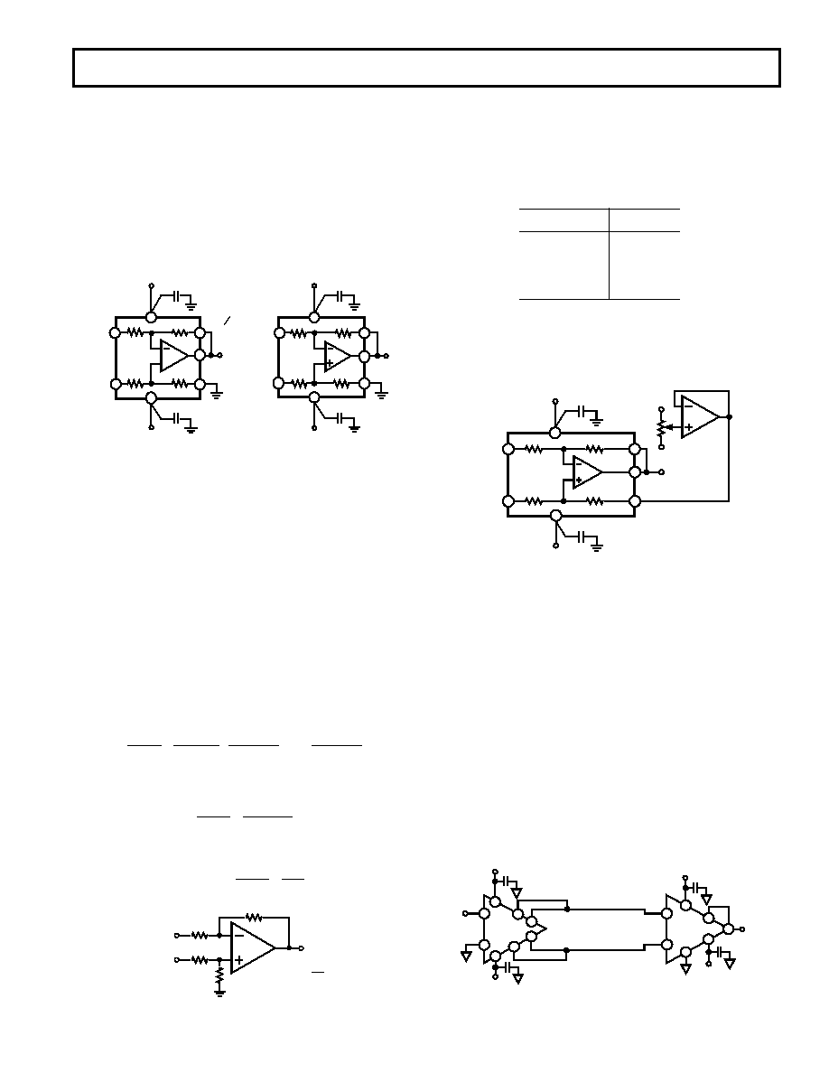
APPLICATIONS INFORMATION
The SSM2143 is designed as a balanced differential line re-
ceiver. It uses a high speed, low noise audio amplifier with four
precision thin-film resistors to maintain excellent common-mode
rejection and ultralow THD. Figure 25 shows the basic differen-
tial receiver application where the SSM2143 yields a gain of 1/2.
The placement of the input and feedback resistors can be
switched to achieve a gain of +2, as shown in Figure 26. For
either circuit configuration, the SSM2143 can also be used un-
balanced by grounding one of the inputs. In applications requir-
ing a gain of +1, use the SSM2141.
6
3
5
1
4
2
7
6k
12k
–IN
+IN
–15V
0.1F
+15V
0.1F
A = 2
V
SSM2143
VOUT
6
1
2
4
5
7
12k
6k
–IN
+IN
–15V
0.1F
VOUT
+15V
0.1F
A =
V
1
2
SSM2143
3
+
Figure 25. Standard Config-
uration for Gain of 1/2
CMRR
The internal thin-film resistors are precisely trimmed to achieve
a CMRR of 90 dB. Any imbalances introduced by the external
circuitry will cause a significant reduction in the overall CMRR
performance. For example, a 5
source imbalance will result in
a CMRR of 71 dB at dc. This is also true for any reactive source
impedances that may affect the CMRR over the audio frequency
range. These error sources need to be minimized to maintain
the excellent CMRR.
To quantify the required accuracy of the thin film resistor
matching, the source of CMRR error can be analyzed. A resistor
mismatch can be modelled as shown in Figure 27. By assuming
a tolerance on one of the 12 k
resistors of R, the equation for
the common-mode gain becomes:
VOUT
VIN
=
6k
+12k
6k
12k
+R
+1
–
6k
12k
+R
which reduces to:
VOUT
VIN
=
1/3
R
12k
+R
This gain error leads to a common-mode rejection ratio of:
CMRR
=
|ADM|
|ACM|
18k
R
–IN
+IN
6k
12k +
R
12k
VOUT
CMRR =
18k
R
Figure 27. A Small Mismatch in Resistance Results in a
Large Common-Mode Error
Setting
R to 5 results in the CMRR of 71 dB, as stated
above. To achieve the SSM2143’s CMRR of 90 dB, the resistor
mismatch can be at most 0.57
. In other words, to build this
circuit discretely, the resistors would have to be matched to
better than 0.005%!
The following table shows typical resistor accuracies and the
resulting CMRR for a differential amplifier.
% Mismatch
CMRR
5%
30 dB
1%
44 dB
0.1%
64 dB
0.005%
90 dB
DC OUTPUT LEVEL ADJUST
The reference node of the SSM2143 is normally connected to
ground. However, it can be used to null out any dc offsets in
the system or to introduce a dc reference level other than
ground. As shown in Figure 28, the reference node needs to be
REFERENCE
OP27
+10V
–10V
6
1
2
3
4
5
7
12k
6k
–IN
+IN
–15V
0.1F
VOUT
+15V
0.1F
SSM2143
Figure 28. A Low Impedance Buffer Is Required to Adjust
the Reference Voltage.
buffered with an op amp to maintain very low impedance to
achieve high CMRR. The same reasoning as above applies such
that the 6 k
resistor has to be matched to better than 0.005%
or 0.3
. The op amp maintains very low output impedance
over the entire audio frequency range, as long as its bandwidth
is well above 20 kHz. The reference input can be adjusted over
a
±10 V range. The gain from the reference to the output is
unity so the resulting dc output adjustment range is also
±10 V.
INPUT ERRORS
The main dc input offset error specified for the SSM2143 is the
Input Offset Voltage. The Input Bias Current and Input Offset
Current are not specified as for a normal operational amplifier.
Because the SSM2143 has built-in resistors, any bias current
related errors are converted into offset voltage errors. Thus, the
offset voltage specification is a combination of the amplifier’s
offset voltage plus its offset current times the input impedance.
Figure 26. Reversing the
Resistors Results in a
Gain of 2
Figure 29. SSM2142/SSM2143 Balanced Line Driver/
Receiver System
2
6
5
4
3
8
7
SSM2142
VIN
SSM2143
+18V
–18V
+18V
0.1F
–18V
VOUT
3
7
6
4
1
2
5
ALL CABLE MEASUREMENTS USE
BELDEN CABLE (500').
1
A
相关PDF资料 |
PDF描述 |
|---|---|
| SY84403BLMG TR | IC AMP LIMIT CML 4.25GBPS 10-MLF |
| SY88303BLMG TR | IC AMP CML LIMITING POST 16MLF |
| SY88305BLMG TR | IC AMP CML LIMITING POST 16MLF |
| SY88307BLMG | IC AMP PECL LIMITING POST 16-MLF |
| SY88309BLMG TR | IC AMP PECL LIMITING POST 16MLF |
相关代理商/技术参数 |
参数描述 |
|---|---|
| SSM2160 | 制造商:AD 制造商全称:Analog Devices 功能描述:6-Channel, Serial Input Master/Balance Volume Controls |
| SSM2160_03 | 制造商:AD 制造商全称:Analog Devices 功能描述:6-Channel, Serial Input Master/Balance Volume Controls |
| SSM2160N | 制造商:未知厂家 制造商全称:未知厂家 功能描述:Tone/Volume/Balance Control |
| SSM2160P | 制造商:Rochester Electronics LLC 功能描述:6 CHANNEL VOLUME CONTROL - Bulk |
| SSM2160R | 制造商:未知厂家 制造商全称:未知厂家 功能描述:Tone/Volume/Balance Control |
发布紧急采购,3分钟左右您将得到回复。