参数资料
| 型号: | SSM2160SZ-REEL |
| 厂商: | Analog Devices Inc |
| 文件页数: | 4/16页 |
| 文件大小: | 0K |
| 描述: | IC CTRLR DGTL VOL/CHAN 24SOIC |
| 产品变化通告: | Product Discontinuance 27/Oct/2011 |
| 标准包装: | 1,000 |
| 类型: | 立体声音量控制 |
| 应用: | 解码器,接收器,环绕系统 |
| 安装类型: | 表面贴装 |
| 封装/外壳: | 24-SOIC(0.295",7.50mm 宽) |
| 供应商设备封装: | 24-SOIC W |
| 包装: | 带卷 (TR) |
REV. A
–12–
SSM2160
DC Blocking and Frequency Response
All internal signal handling uses direct coupled circuitry. Although
the input and output dc offsets are small, dc blocking is required
when the signal ground references are different. This will be the
case if the source is from an op amp that uses dual power supplies
(i.e.,
±6 V), and the SSM2160 uses a single supply. If the signal
source has the capability of operating with an externally supplied
signal, connect the VREF (Pin 3) to the source’s external ground
input either directly or through a buffer as shown in Figure 4.
The same consideration is applied to the load. If the load is
returned to AGND, no capacitor is required. When the SSM2160
is operated from a single supply, there will be a dc output level
of +VS/2 at the output. This will require dc blocking capacitors
if driving a load referred to GND.
When dc blocking capacitors are used at the inputs and outputs,
they form a high-pass filter with the input and load resistance,
both of which are typically 10 k
. To calculate the lower –3 dB
frequency of the high-pass filter formed by the coupling capacitor
and the input resistance, use either of the following formulas
fRC
or
CRf
C
=
()
=
()
12
π
where
R is the typically 10 k
input resistance of the SSM2160 or the
load resistance. C is the value of the blocking capacitor when fC
is known.
If a cutoff frequency of 20 Hz were desired, solving for C gives
0.8
F for the input or output capacitor. A higher load imped-
ance will allow smaller output capacitors to give the same 20 Hz
cutoff. Note that the overall low-pass filter will be the cascade of
the two, so the response will be –6 dB at 20 Hz. A practical and
economical choice would be 1
F/15 V electrolytics.
Signal/Noise Considerations and Channel Center Gain
The SSM2160 should be placed in the signal flow where levels
are high enough to result in low distortion and good SNR but
not so high to require unusually high power supplies. In a typical
application, input and output signal levels will be in the 300 mV
± 200 mV rms range. This level is typically available from internal
and external sources. As previously mentioned, the 31 dB of
gain available in the VCA is usually used for balancing the various
channels and is usually set to 15 dB or 16 dB in its center posi-
tion. Due to the nature of VCA performance versus gain, the
minimum gain that will allow balancing the channels should be
used. If no balance function is required, the channel gain should
be set to 0 dB. Use the lowest value of centered gain when less
than the full balance range is needed. For example, if only
±6 dB
channel gain variations were needed, the center could be set at
6 dB, giving 6 dB
± 6 dB, rather than at 15 dB ± 6 dB. This
would result in improved S/N ratio and less distortion.
Digital Interface
Digital logic signals have fast rising and falling edges that can
easily be coupled into the signal and ground paths if care is not
taken with PC board trace routing, ground management, and
proper bypassing. In addition, limiting the high state logic signal
levels to 3.5 V will minimize noise coupling.
Load Considerations
The output of each SSM2160 channel must be loaded with a mini-
mum of 10 k
. Connecting a load of less than 10 k will result
in increased distortion and may cause excessive internal heating
with possible damage to the device. Capacitive loading should be
kept to less than 50 pF. Excessive capacitive loading may increase
the distortion level and may cause instability in the output ampli-
fiers. If your application requires driving a lower impedance or
more capacitive load, use a buffer as shown in Figure 12.
CH6 OUT
SSM2160
CH1 OUT
CH6 OUT
1/2 SSM2135
CH1 OUT
Figure 12. Output Buffers to Drive Capacitive Loads
Windows Software
Windows software is available to customers from Analog Devices
to interface the serial port of a PC (running Windows 3.1 or
higher) with the SSM2160. Contact your sales representative for
details on obtaining the software. For details, see the Evaluation
Board section.
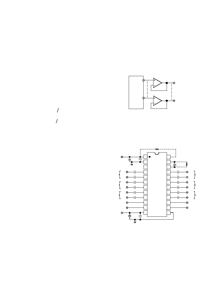
13
16
15
14
23
22
21
20
19
18
17
12
11
10
9
8
1
2
3
4
7
6
5
SSM2160
+
0.1 F
10F
+
0.1 F
10 F
+
10 F
RM*
OUT
IN
CH 2
OUT
IN
CH 4
OUT
IN
CH 6
DATA
CLK
OUT
IN
CH 1
OUT
IN
CH 3
OUT
IN
CH 5
V–
WRITE
LD
V+
**OPTIONAL SEE “CHANNEL STEP SIZE”
**TYPICAL 1 F–10 F: SEE “DC BLOCKING AND FREQUENCY RESPONSE”
RC*
**
Figure 13. Typical Application Circuit (Dual Supply)
相关PDF资料 |
PDF描述 |
|---|---|
| SSM2166SZ | IC PREAMP AUDIO MONO MIC 14SOIC |
| SSM2167-1RMZ-R7 | IC PREAMP AUDIO MONO AB 10MSOP |
| SSM2301CPZ-R2 | IC AMP AUDIO 1.52W MONO D 8LFCSP |
| SSM2302CPZ-R2 | IC AMP AUDIO 1.4W STER D 16LFCSP |
| SSM2304CPZ-REEL7 | IC AMP AUDIO 2.4W STER D 16LFCSP |
相关代理商/技术参数 |
参数描述 |
|---|---|
| SSM2161 | 制造商:AD 制造商全称:Analog Devices 功能描述:6- and 4-Channel, Serial Input Master/Balance Volume Controls |
| SSM2161N | 制造商:未知厂家 制造商全称:未知厂家 功能描述:Tone/Volume/Balance Control |
| SSM2161P | 制造商:AD 制造商全称:Analog Devices 功能描述:6- and 4-Channel, Serial Input Master/Balance Volume Controls |
| SSM2161R | 制造商:未知厂家 制造商全称:未知厂家 功能描述:Tone/Volume/Balance Control |
| SSM2161S | 制造商:AD 制造商全称:Analog Devices 功能描述:6- and 4-Channel, Serial Input Master/Balance Volume Controls |
发布紧急采购,3分钟左右您将得到回复。