- 您现在的位置:买卖IC网 > PDF目录16602 > SSM2167Z-EVAL (Analog Devices Inc)BOARD EVAL FOR SSM2167 PDF资料下载
参数资料
| 型号: | SSM2167Z-EVAL |
| 厂商: | Analog Devices Inc |
| 文件页数: | 11/12页 |
| 文件大小: | 0K |
| 描述: | BOARD EVAL FOR SSM2167 |
| 标准包装: | 1 |
| 主要目的: | 音频,麦克风前置放大器 |
| 嵌入式: | 否 |
| 已用 IC / 零件: | SSM2167 |
| 主要属性: | 可变压缩,噪音选通,0.2% THD + N,可调式压缩比 |
| 次要属性: | 自动限制性能可防止 ADC 过载,3 V(2.5 ~ 5.5 V) |
| 已供物品: | 板 |
| 产品目录页面: | 775 (CN2011-ZH PDF) |
| 相关产品: | SSM2167-1RMZ-REELDKR-ND - IC PREAMP AUDIO MONO AB 10MSOP SSM2167-1RMZ-REELCT-ND - IC PREAMP AUDIO MONO AB 10MSOP SSM2167-1RMZ-REELTR-ND - IC PREAMP AUDIO MONO AB 10MSOP |
SSM2167
Data Sheet
Rev. G | Page 8 of 12
APPLICATIONS INFORMATION
The SSM2167 is a complete microphone signal conditioning
system on a single integrated circuit. Designed primarily for
voice-band applications, this integrated circuit provides ampli-
fication, limiting, variable compression, and noise gate. User
adjustable compression ratio, noise gate threshold, and two
different fixed gains optimize circuit operation for a variety of
applications. The SSM2167 also features a low power shutdown
mode for battery-powered applications.
10
1
2
4
3
9
7
8
5
6
+
SSM2167
10F
GND
VDD
500k
SHUTDOWN
INPUT
0.1F
10F
+
10F
GND
RCOMP
RGATE
100k
OUTPUT
+
10F
02628-
016
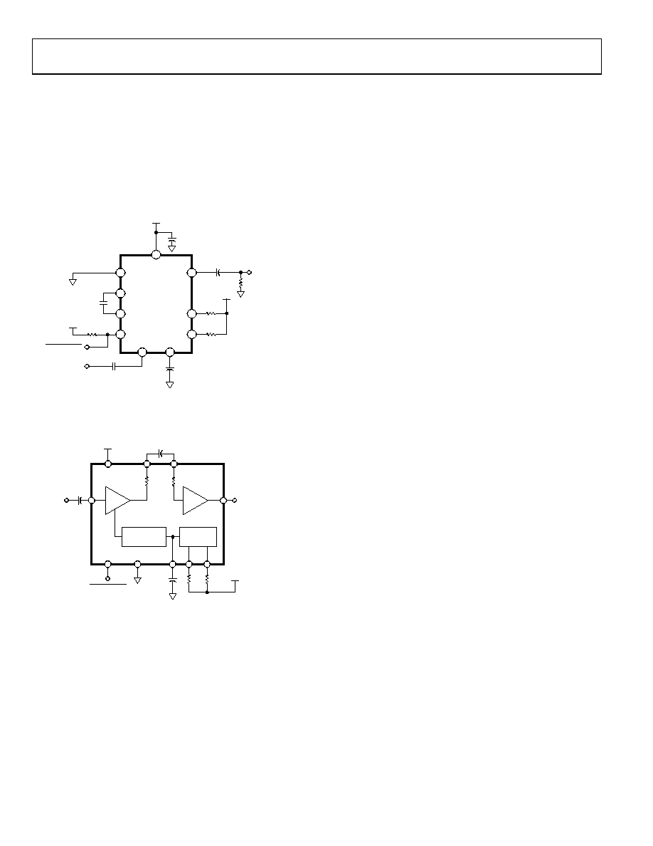
Figure 15. Typical Application Circuit
VCA
+1
CONTROL
C1
0.1F
+
C2
10F
1k
OUTPUT
NOISE GATE AND
COMPRESSION
SETTINGS
LEVEL
DETECTOR
BUFFER
+
INPUT
GND
+
CAVG
C3
10F
SHUTDOWN
RC
RG
VDD
BUFOUT
VCAIN
02628-
017
Figure 16. Functional Block Diagram
THEORY OF OPERATION
The typical transfer characteristic for the SSM2167 is shown in
Figure 2 where the output level in dB is plotted as a function of
the input level in dB. The dotted line indicates the transfer char-
acteristic for a unity-gain amplifier. For input signals in the range
of VDE (downward expansion) to VRP (rotation point), an “r” dB
change in the input level causes a 1 dB change in the output level.
Here, r is defined as the compression ratio. The compression ratio
may be varied from 1:1 (no compression) to 10:1 via a single
resistor, RCOMP. Input signals above VRP are compressed with a
fixed compression ratio of approximately 10:1. This region of
operation is the limiting region. Varying the compression ratio
has no effect on the limiting region.
The breakpoint between the compression region and the limiting
region is referred to as the limiting threshold or the rotation point.
The term, rotation point, derives from the observation that the
straight line in the compression region rotates about this point on
the input/output characteristic as the compression ratio is changed.
The gain of the system with an input signal level of VRP is the fixed
gain, 18 dBV for the SSM2167, regardless of the compression ratio.
Input signals below VDE are downward expanded; that is, a
1 dB change in the input signal level causes approximately a
3 dB change in the output level. As a result, the gain of the
system is small for very small input signal levels, even though
it may be quite large for small input signals above VDE. The
external resistor at Pin 7, RGATE, is used to set the downward
expansion threshold (VDE).
Finally, the SSM2167 provides an active low, CMOS-compatible
digital power-down feature that reduces device supply current
to typically less than 2 A.
SIGNAL PATH
Figure 16 illustrates the block diagram of the SSM2167. The
audio input signal is processed by the input buffer and then by
the VCA. The input buffer presents an input impedance of
approximately 100 kΩ to the source. A dc voltage of approximately
400 mV is present at INPUT (Pin 5) of the SSM2167, requiring the
use of a blocking capacitor (C1) for ground-referenced sources.
A 0.1 F capacitor is a good choice for most audio applications.
The input buffer is a unity-gain stable amplifier that can drive
the low impedance input of the VCA and an internal rms detector.
The VCA is a low distortion, variable gain amplifier whose gain
is set by the side-chain control circuitry. An external blocking
capacitor (C2) must be used between the buffer output and the
VCA input. The 1 kΩ impedance between amplifiers determines
the value of this capacitor, which is typically between 4.7 F and
10 F. An aluminum electrolytic capacitor is an economical choice.
The VCA amplifies the input signal current flowing through C2
and converts this current to a voltage at the output pin (Pin 9) of
the SSM2167. The net gain from input to output can be as high
as 40 dB, depending on the gain set by the control circuitry.
The output impedance of the SSM2167 is typically less than
145 Ω, and the external load on Pin 9 should be >5 kΩ. The
nominal output dc voltage of the device is approximately 1.4 V;
therefore, a blocking capacitor for grounded loads must be used.
The bandwidth of the SSM2167 is quite wide at all gain settings.
The upper 3 dB point is over 1 MHz at gains as high as 30 dB.
The GBW plots are shown in Figure 5. The lower 3 dB cutoff
frequency of the SSM2167 is set by the input impedance of the
VCA (1 kΩ) and C2. Whereas the noise of the input buffer is
fixed, the input-referred noise of the VCA is a function of gain.
The VCA input noise is designed to be at a minimum when the
gain is at a maximum, thereby maximizing the usable dynamic
range of the part.
相关PDF资料 |
PDF描述 |
|---|---|
| RCE05DHFD | CONN EDGECARD 10POS 1MM SMD |
| TC646BEPA | IC PWM FAN SPEED CTRLR SD 8-DIP |
| EEC49DRYN | CONN EDGECARD 98POS DIP .100 SLD |
| RBE05DHFD | CONN EDGECARD 10POS 1MM SMD |
| 1SMA5929BT3 | DIODE ZENER 15V 1.5W SMA |
相关代理商/技术参数 |
参数描述 |
|---|---|
| SSM2167Z-EVAL | 制造商:Analog Devices 功能描述:SSM2167, MICROPHONE PREAMPLIFIER, EVALUA |
| SSM-21T-P1.4 | 制造商:JST Manufacturing 功能描述:N/R 1 N/R s Straight 17.6mm Crimp 300VDC / 300VAC 7A 105 -40 Tin 制造商:JST Manufacturing 功能描述:Phosphor Bronze Tin Plated Pin Contact |
| SSM22001MYB | 制造商:SHELLY ASSOCIATES 功能描述: |
| SSM2210 | 制造商:AD 制造商全称:Analog Devices 功能描述:Audio Dual Natched NPN transistor |
| SSM-2210 | 制造商:AD 制造商全称:Analog Devices 功能描述:Audio Dual Natched NPN transistor |
发布紧急采购,3分钟左右您将得到回复。