- 您现在的位置:买卖IC网 > PDF目录10399 > SSM2804CBZ-RL (Analog Devices Inc)IC AMP AUDIO DR 30-WLSCP PDF资料下载
参数资料
| 型号: | SSM2804CBZ-RL |
| 厂商: | Analog Devices Inc |
| 文件页数: | 5/36页 |
| 文件大小: | 0K |
| 描述: | IC AMP AUDIO DR 30-WLSCP |
| 标准包装: | 1 |
| 类型: | D 类 |
| 输出类型: | 2-通道(立体声)带立体声耳机 |
| 在某负载时最大输出功率 x 通道数量: | 3.6W x 2 @ 4 欧姆; 40mW x 2 @ 16 欧姆 |
| 电源电压: | 2.5 V ~ 3.6 V |
| 特点: | 消除爆音,I²C,短路和热保护,关机,音量控制 |
| 安装类型: | 表面贴装 |
| 供应商设备封装: | 30-WLCSP(2.96x2.46) |
| 封装/外壳: | 30-WFBGA,WLBGA |
| 包装: | 标准包装 |
| 其它名称: | SSM2804CBZ-RLDKR |
第1页第2页第3页第4页当前第5页第6页第7页第8页第9页第10页第11页第12页第13页第14页第15页第16页第17页第18页第19页第20页第21页第22页第23页第24页第25页第26页第27页第28页第29页第30页第31页第32页第33页第34页第35页第36页
SSM2804
Rev. 0 | Page 13 of 36
THEORY OF OPERATION
The SSM2804 audio subsystem features a filterless modulation
scheme that greatly reduces the external component count, con-
serving board space and, thus, reducing system cost. The SSM2804
does not require an output filter but, instead, relies on the inherent
inductance of the speaker coil and the natural filtering of the
speaker and human ear to fully recover the audio component
of the square wave output.
Most Class-D amplifiers use some variation of pulse-width
modulation (PWM), but the SSM2804 uses Σ-Δ modulation to
determine the switching pattern of the output devices, resulting
in a number of important benefits.
Σ-Δ modulators do not produce a sharp peak with many
harmonics in the AM frequency band, as pulse-width
modulators often do.
Σ-Δ modulation provides the benefits of reducing the
amplitude of spectral components at high frequencies,
that is, reducing EMI emissions that might otherwise
be radiated by speakers and long cable traces.
The SSM2804 does not require external EMI filtering for
twisted speaker cable lengths shorter than 10 cm. If longer
speaker cables are used, the SSM2804 has emission limiting
circuitry that allows significantly longer speaker cable.
Due to the inherent spread-spectrum nature of Σ-Δ modu-
lation, the need for modulator synchronization is eliminated
for designs that incorporate multiple SSM2804 amplifiers.
be selected from a range of +12 dB to 63 dB in 32 steps. Other
features accessed from the I2C interface include the following:
Independent left/right channel shutdown
Variable ultralow EMI emission limiting circuitry
Automatic level control (ALC) for high quality speaker
protection
Stereo-to-mono mixing operation
The SSM2804 also offers protection circuits for overcurrent and
overtemperature protection.
POP-AND-CLICK SUPPRESSION
Voltage transients at the output of audio amplifiers can occur
when shutdown is activated or deactivated. Voltage transients
as low as 10 mV can be heard as an audio pop in the speaker.
Clicks and pops can also be classified as undesirable audible
transients generated by the amplifier system and, therefore, as
not coming from the system input signal. Such transients may
be generated when the amplifier system changes its operating
mode. For example, the following may be sources of audible
transients: system power-up and power-down, mute and
unmute, input source change, and sample rate change.
The SSM2804 has a pop-and-click suppression architecture that
reduces these output transients, resulting in noiseless activation
and deactivation.
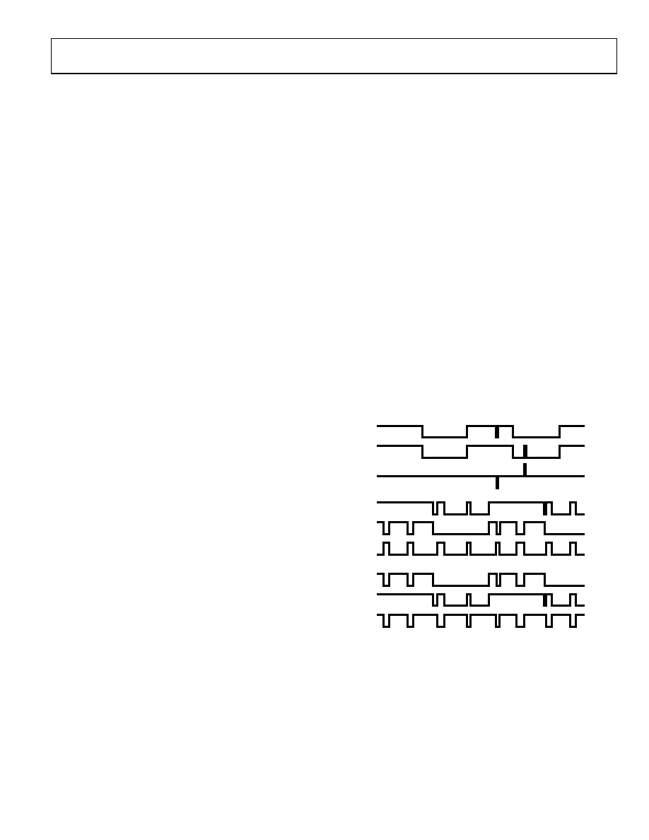
OUTPUT MODULATION DESCRIPTION
The SSM2804 uses three-level, Σ-Δ output modulation. Each
output can swing from GND to VDD and vice versa. Ideally, when
no input signal is present, the output differential voltage is 0 V
because there is no need to generate a pulse. In a real-world
situation, noise sources are always present.
Due to the constant presence of noise, a differential pulse is
generated, when required, in response to this stimulus. A small
amount of current flows into the inductive load when the differ-
ential pulse is generated.
Most of the time, however, the output differential voltage is 0 V,
due to the Analog Devices, Inc., three-level, Σ-Δ output modu-
lation. This feature ensures that the current flowing through the
inductive load is small.
When the user wants to send an input signal, an output pulse
(OUT+ and OUT) is generated to follow the input voltage.
The differential pulse density (VOUT) is increased by raising the
input signal level. Figure 28 depicts three-level, Σ-Δ output
modulation with and without input stimulus.
OUTPUT > 0V
+5V
0V
OUT+
+5V
0V
OUT–
+5V
0V
VOUT
OUTPUT < 0V
+5V
0V
OUT+
+5V
0V
OUT–
0V
–5V
VOUT
OUTPUT = 0V
OUT+
+5V
0V
+5V
0V
OUT–
+5V
–5V
0V
VOUT
09
96
0-
1
04
Figure 28. Three-Level, Σ-Δ Output Modulation
With and Without Input Stimulus
相关PDF资料 |
PDF描述 |
|---|---|
| VI-J7T-MY-B1 | CONVERTER MOD DC/DC 6.5V 50W |
| MS27484T12B3SLC | CONN HSG PLUG 3POS STRGHT SCKT |
| MS27484T8F35B | CONN HSG PLUG 6POS STRGHT SCKT |
| VI-J7R-MY-B1 | CONVERTER MOD DC/DC 7.5V 50W |
| VI-J7P-MY-B1 | CONVERTER MOD DC/DC 13.8V 50W |
相关代理商/技术参数 |
参数描述 |
|---|---|
| SSM28APT | 制造商:CHENMKO 制造商全称:Chenmko Enterprise Co. Ltd. 功能描述:SCHOTTKY BARRIER RECTIFIER |
| SSM28G45EM | 制造商:SSC 制造商全称:Silicon Standard Corp. 功能描述:N-CHANNEL INSULATED-GATE BIPOLAR TRANSISTOR |
| SSM28PT | 制造商:CHENMKO 制造商全称:Chenmko Enterprise Co. Ltd. 功能描述:SCHOTTKY BARRIER RECTIFIER |
| SSM2932 | 制造商:AD 制造商全称:Analog Devices 功能描述:High Efficiency, Ground-Referenced |
| SSM2932ACBZ | 制造商:Analog Devices 功能描述:AMP CLASS G STEREO 0.1W 16WLCSP 制造商:Analog Devices 功能描述:AMP, CLASS G, STEREO, 0.1W, 16WLCSP |
发布紧急采购,3分钟左右您将得到回复。