- 您现在的位置:买卖IC网 > PDF目录271213 > SST55LC100-45-I-BWE FLASH MEMORY DRIVE CONTROLLER, PBGA84 PDF资料下载
参数资料
| 型号: | SST55LC100-45-I-BWE |
| 元件分类: | 存储控制器/管理单元 |
| 英文描述: | FLASH MEMORY DRIVE CONTROLLER, PBGA84 |
| 封装: | ROHS COMPLIANT, MO-210, TFBGA-84 |
| 文件页数: | 18/80页 |
| 文件大小: | 758K |
| 代理商: | SST55LC100-45-I-BWE |
第1页第2页第3页第4页第5页第6页第7页第8页第9页第10页第11页第12页第13页第14页第15页第16页第17页当前第18页第19页第20页第21页第22页第23页第24页第25页第26页第27页第28页第29页第30页第31页第32页第33页第34页第35页第36页第37页第38页第39页第40页第41页第42页第43页第44页第45页第46页第47页第48页第49页第50页第51页第52页第53页第54页第55页第56页第57页第58页第59页第60页第61页第62页第63页第64页第65页第66页第67页第68页第69页第70页第71页第72页第73页第74页第75页第76页第77页第78页第79页第80页
Advance Information
CompactFlash Card Controller
SST55LC100
2005 Silicon Storage Technology, Inc.
S71298-00-000
10/05
25
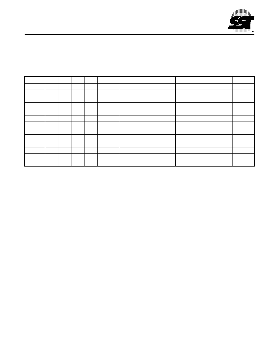
9.1.2 Contiguous I/O Mapped Addressing
When the system decodes a contiguous block of I/O registers to select the CompactFlash card, the registers are
accessed in the block of I/O space decoded by the system as follows:
Note: Address lines which are not indicated are ignored by the CompactFlash card for accessing all the registers in this table.
TABLE
9-3: CONTIGUOUS I/O DECODING
REG#
A3
A2
A1
A0
Offset
IORD#=0
IOWR#=0
Notes
0
0000
0
Even RD Data
Even WR Data
1
1. Register 0 is accessed with CE1# low and CE2# low (and A0 = Don’t Care) as a word register on the combined Odd Data Bus and
Even Data Bus (D15-D0). This register may also be accessed by a pair of byte accesses to the offset 0 with CE1# low and CE2#
high. Note that the address space of this word register overlaps the address space of the Error and Feature byte-wide registers that
lie at offset 1. When accessed twice as byte register with CE1# low, the first byte to be accessed is the Even Byte of the word and the
second byte accessed is the Odd Byte of the equivalent word access. A byte access to register 0 with CE1# high and CE2# low
accesses the error (read) or feature (write) register.
0
0001
1
Error
Features
2
2. Registers at offset 8, 9, and D are non-overlapping duplicates of the registers at offset 0 and 1.
Register 8 is equivalent to register 0, while register 9 accesses the Odd Byte. Therefore, if the registers are byte accessed in the
order 9 then 8 the data will be transferred Odd Byte then Even Byte.
Repeated byte accesses to register 8 or 0 will access consecutive (Even then Odd) Bytes from the data buffer. Repeated word
accesses to register 8, 9, or 0 will access consecutive words from the data buffer. Repeated byte accesses to register 9 are not sup-
ported. However, repeated alternating byte accesses to registers 8 then 9 will access consecutive (Even then Odd) Bytes from the
data buffer. Byte accesses to register 9 access only the Odd Byte of the data.
0
0010
2
Sector Count
0
0011
3
Sector No.
0
0100
4
Cylinder Low
0
0101
5
Cylinder High
0
0110
6
Select Card/Head
0
0111
7
Status
Command
0
1000
8
Dup. Even RD Data
Dup. Even WR Data
0
1001
9
Dup. Odd RD Data
Dup. Odd WR Data
0
1101
D
Dup. Error
Dup. Features
0
1110
E
Alt Status
Device Ctl
0
1111
F
Drive Address
Reserved
T9-3.0 1298
相关PDF资料 |
PDF描述 |
|---|---|
| ST7FLITE19BF0B6 | 8-BIT, FLASH, 8 MHz, MICROCONTROLLER, PDIP20 |
| ST7PLITE15BF0B3 | 8-BIT, MROM, 8 MHz, MICROCONTROLLER, PDIP20 |
| STR711FR0H3 | 32-BIT, FLASH, 66 MHz, RISC MICROCONTROLLER, PBGA64 |
| STR711FRH3 | 32-BIT, FLASH, 66 MHz, RISC MICROCONTROLLER, PBGA64 |
| STR711FZ2H3TR | 32-BIT, FLASH, 66 MHz, RISC MICROCONTROLLER, PBGA144 |
相关代理商/技术参数 |
参数描述 |
|---|---|
| SST55LC100-45-I-TQWE | 制造商:SST 制造商全称:Silicon Storage Technology, Inc 功能描述:CompactFlash Card Controller |
| SST55LC100M | 制造商:SST 制造商全称:Silicon Storage Technology, Inc 功能描述:CompactFlash Card Controller |
| SST55LC100M-45-C-BWE | 功能描述:总线收发器 Compact Flash 45MHz 3.3V Commercial RoHS:否 制造商:Fairchild Semiconductor 逻辑类型:CMOS 逻辑系列:74VCX 每芯片的通道数量:16 输入电平:CMOS 输出电平:CMOS 输出类型:3-State 高电平输出电流:- 24 mA 低电平输出电流:24 mA 传播延迟时间:6.2 ns 电源电压-最大:2.7 V, 3.6 V 电源电压-最小:1.65 V, 2.3 V 最大工作温度:+ 85 C 封装 / 箱体:TSSOP-48 封装:Reel |
| SST55LC100M-45-C-TQWE | 功能描述:总线收发器 Compact Flash 45MHz 3.3V Commercial RoHS:否 制造商:Fairchild Semiconductor 逻辑类型:CMOS 逻辑系列:74VCX 每芯片的通道数量:16 输入电平:CMOS 输出电平:CMOS 输出类型:3-State 高电平输出电流:- 24 mA 低电平输出电流:24 mA 传播延迟时间:6.2 ns 电源电压-最大:2.7 V, 3.6 V 电源电压-最小:1.65 V, 2.3 V 最大工作温度:+ 85 C 封装 / 箱体:TSSOP-48 封装:Reel |
| SST55LC100M-45-I-BWE | 制造商:SST 制造商全称:Silicon Storage Technology, Inc 功能描述:CompactFlash Card Controller |
发布紧急采购,3分钟左右您将得到回复。