- 您现在的位置:买卖IC网 > PDF目录98142 > SST55LD017D-40-I-TQW (SILICON STORAGE TECHNOLOGY INC) FLASH MEMORY DRIVE CONTROLLER, PQFP100 PDF资料下载
参数资料
| 型号: | SST55LD017D-40-I-TQW |
| 厂商: | SILICON STORAGE TECHNOLOGY INC |
| 元件分类: | 存储控制器/管理单元 |
| 英文描述: | FLASH MEMORY DRIVE CONTROLLER, PQFP100 |
| 封装: | TQFP-100 |
| 文件页数: | 59/59页 |
| 文件大小: | 702K |
| 代理商: | SST55LD017D-40-I-TQW |
第1页第2页第3页第4页第5页第6页第7页第8页第9页第10页第11页第12页第13页第14页第15页第16页第17页第18页第19页第20页第21页第22页第23页第24页第25页第26页第27页第28页第29页第30页第31页第32页第33页第34页第35页第36页第37页第38页第39页第40页第41页第42页第43页第44页第45页第46页第47页第48页第49页第50页第51页第52页第53页第54页第55页第56页第57页第58页当前第59页
EOL Product Document
ATA Flash Disk Controller
SST55LD017D
9
2006 Silicon Storage Technology, Inc.
S71225-01-EOL
4/06
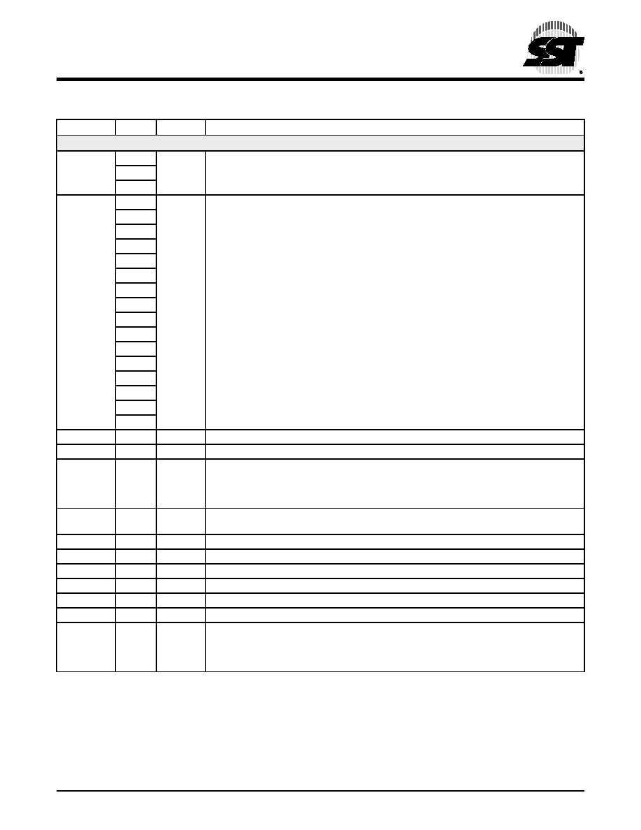
TABLE
3-1: PIN ASSIGNMENTS (1 OF 3)
Symbol
Pin No. I/O Type1 Name and Functions
Host Side Interface
A2
83
I2D
A[2:0] are used to select one of eight registers in the Task File.
A1
84
A0
85
D15
92
I2D/O4
D[15:0] Data bus
D14
59
D13
57
D12
54
D11
52
D10
100
D9
98
D8
95
D7
93
D6
58
D5
56
D4
53
D3
51
D2
99
D1
97
D0
94
CS1FX#
66
I3U
CS1FX# is the chip select for the task file registers.
CS3FX#
67
I3U
CS3FX# is used to select the Alternate Status register and the Device Control register.
CSEL
61
I1U
This internally pulled-up signal is used to configure this device as a Master or a Slave.
When this pin is grounded, this device is configured as a Master. When the pin is open,
this device is configured as a Slave. The pin setting should remain the same from power-
up to power-down.
IORD#
70
I3U
I/O Read strobe generated by the host
This signal gates I/O data onto the bus from the chip.
IOWR#
73
I3U
The I/O Write strobe pulse is used to clock I/O data into the chip.
IOCS16#
90
O4
This output signal is asserted low when the device is indicating a word data transfer cycle.
INTRQ
65
O2
This signal is the active high Interrupt Request to the host.
PDIAG#
89
I2U/O2
The Pass Diagnostic signal in the Master/Slave handshake protocol.
DASP#
63
I2U/O2
The Drive Active/Slave Present signal in the Master/Slave handshake protocol.
RESET#
81
I4U
This input pin is the active low hardware reset from the host.
WP_PD#
62
I2U
The WP_PD# pin can be used for either the Write-Protect mode or Power-Down mode,
but only one mode is active at any time. The Write-Protect or Power-Down modes can be
selected through the host command. The Write-Protect mode is the factory default setting.
For details, please refer to Section 8.0 and Section 11.2.1.18.
相关PDF资料 |
PDF描述 |
|---|---|
| SST55LD019A-45-C-TQPE | FLASH MEMORY DRIVE CONTROLLER, PQFP64 |
| SST55LD019C-45-I-BWE | FLASH MEMORY DRIVE CONTROLLER, PBGA84 |
| SST55LD019B-45-C-TQW | FLASH MEMORY DRIVE CONTROLLER, PQFP100 |
| SST55LD019C-45-C-BWE | FLASH MEMORY DRIVE CONTROLLER, PBGA84 |
| SST55LD019A-45-C-TQP | FLASH MEMORY DRIVE CONTROLLER, PQFP64 |
相关代理商/技术参数 |
参数描述 |
|---|---|
| SST55LD019 | 制造商:SST 制造商全称:Silicon Storage Technology, Inc 功能描述:ATA Flash Disk Controller |
| SST55LD019A | 制造商:SST 制造商全称:Silicon Storage Technology, Inc 功能描述:ATA Flash Disk Controller |
| SST55LD019A-45-C-BWE | 功能描述:总线收发器 ATA Media 45MHz 3.3V Commercial RoHS:否 制造商:Fairchild Semiconductor 逻辑类型:CMOS 逻辑系列:74VCX 每芯片的通道数量:16 输入电平:CMOS 输出电平:CMOS 输出类型:3-State 高电平输出电流:- 24 mA 低电平输出电流:24 mA 传播延迟时间:6.2 ns 电源电压-最大:2.7 V, 3.6 V 电源电压-最小:1.65 V, 2.3 V 最大工作温度:+ 85 C 封装 / 箱体:TSSOP-48 封装:Reel |
| SST55LD019A-45-C-MVWE | 制造商:SST 制造商全称:Silicon Storage Technology, Inc 功能描述:ATA Flash Disk Controller |
| SST55LD019A-45-C-TQWE | 功能描述:总线收发器 ATA Media 45MHz 3.3V Commercial RoHS:否 制造商:Fairchild Semiconductor 逻辑类型:CMOS 逻辑系列:74VCX 每芯片的通道数量:16 输入电平:CMOS 输出电平:CMOS 输出类型:3-State 高电平输出电流:- 24 mA 低电平输出电流:24 mA 传播延迟时间:6.2 ns 电源电压-最大:2.7 V, 3.6 V 电源电压-最小:1.65 V, 2.3 V 最大工作温度:+ 85 C 封装 / 箱体:TSSOP-48 封装:Reel |
发布紧急采购,3分钟左右您将得到回复。