参数资料
| 型号: | ST16C552IJ68TR-F |
| 厂商: | Exar Corporation |
| 文件页数: | 15/39页 |
| 文件大小: | 0K |
| 描述: | IC UART FIFO 16B DUAL 68PLCC |
| 标准包装: | 250 |
| 特点: | * |
| 通道数: | 2,DUART |
| FIFO's: | 16 字节 |
| 规程: | 打印机 |
| 电源电压: | 2.97 V ~ 5.5 V |
| 带并行端口: | 是 |
| 带故障启动位检测功能: | 是 |
| 带调制解调器控制功能: | 是 |
| 带CMOS: | 是 |
| 安装类型: | 表面贴装 |
| 封装/外壳: | 68-LCC(J 形引线) |
| 供应商设备封装: | 68-PLCC |
| 包装: | 带卷 (TR) |
第1页第2页第3页第4页第5页第6页第7页第8页第9页第10页第11页第12页第13页第14页当前第15页第16页第17页第18页第19页第20页第21页第22页第23页第24页第25页第26页第27页第28页第29页第30页第31页第32页第33页第34页第35页第36页第37页第38页第39页
22
ST16C552/552A
Rev. 3.40
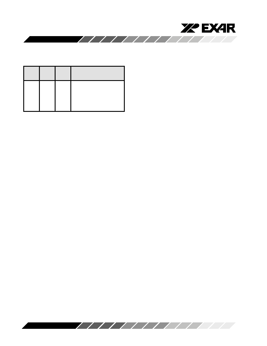
LCR
Parity selection
Bit-5
Bit-4
Bit-3
X
0
No parity
0
1
Odd parity
0
1
Even parity
1
0
1
Force parity odd parity
1
Forced even parity
LCR BIT-6:
When enabled the Break control bit causes a break
condition to be transmitted (the TX output is forced to
a logic 0 state). This condition exists until disabled by
setting LCR bit-6 to a logic 0.
Logic 0 = No TX break condition. (normal default
condition)
Logic 1 = Forces the transmitter output (TX) to a logic
0 for alerting the remote receiver to a line break
condition.
LCR BIT-7:
The internal baud rate counter latch and Enhance
Feature mode enable.
Logic 0 = Divisor latch disabled. (normal default
condition)
Logic 1 = Divisor latch and enhanced feature register
enabled.
Modem Control Register (MCR)
This register controls the interface with the modem or
a peripheral device.
MCR BIT-0:
Logic 0 = Force -DTR output to a logic 1. (normal
default condition)
Logic 1 = Force -DTR output to a logic 0.
MCR BIT-1:
Logic 0 = Force -RTS output to a logic 1. (normal
default condition)
Logic 1 = Force -RTS output to a logic 0.
MCR BIT-2:
This bit is used in the Loop-back mode only. In the
loop-back mode this bit is use to write the state of the
modem -RI interface signal.
MCR BIT-3: (Used to control the modem -CD signal
in the loop-back mode.)
Logic 0 = Forces INT (A-B) outputs to the three state
mode. (normal default condition) In the Loop-back
mode, sets -CD internally to a logic 1.
Logic 1 = Forces the INT (A-B) outputs to the active
mode. In the Loop-back mode, sets -CD internally to
a logic 0.
MCR BIT-4:
Logic 0 = Disable loop-back mode. (normal default
condition)
Logic 1 = Enable local loop-back mode (diagnostics).
MCR BIT 5-6:
Not Used - initialized to a logic 0.
MCR BIT-7:
Logic 0 = Disable power down mode. (normal, default
condition, 552 only)
Logic 1 = Enable power down mode (IER bit-5 must
also be a logic 1 before power down will be activated).
Line Status Register (LSR)
This register provides the status of data transfers
between. the 552/552A and the CPU.
LSR BIT-0:
Logic 0 = No data in receive holding register or FIFO.
(normal default condition)
Logic 1 = Data has been received and is saved in the
receive holding register or FIFO.
LSR BIT-1:
Logic 0 = No overrun error. (normal default condition)
Logic 1 = Overrun error. A data overrun error occurred
in the receive shift register. This happens when addi-
tional data arrives while the FIFO is full. In this case
the previous data in the shift register is overwritten.
Note that under this condition the data byte in the
receive shift register is not transferred into the FIFO,
therefore the data in the FIFO is not corrupted by the
error.
相关PDF资料 |
PDF描述 |
|---|---|
| ST16C554DIQ64TR-F | IC UART FIFO 16B QUAD 64LQFP |
| ST16C580IQ48-F | IC UART FIFO 16B 48TQFP |
| ST16C650AIJ44-F | IC UART FIFO 32B 44PLCC |
| ST16C654DIQ64-F | IC UART FIFO 64B QUAD 64LQFP |
| ST78C34CJ44-F | IC UART FIFO 83B 44PLCC |
相关代理商/技术参数 |
参数描述 |
|---|---|
| ST16C554 | 制造商:EXAR 制造商全称:EXAR 功能描述:2.97V TO 5.5V QUAD UART WITH 16-BYTE FIFO |
| ST16C554CJ-0A-EVB | 功能描述:界面开发工具 Supports C554D 68 ld PLCC, ISA Interface RoHS:否 制造商:Bourns 产品:Evaluation Boards 类型:RS-485 工具用于评估:ADM3485E 接口类型:RS-485 工作电源电压:3.3 V |
| ST16C554CQ-0A-EVB | 功能描述:界面开发工具 Supports C554 64 ld TQFP, ISA Interface RoHS:否 制造商:Bourns 产品:Evaluation Boards 类型:RS-485 工具用于评估:ADM3485E 接口类型:RS-485 工作电源电压:3.3 V |
| ST16C554CQ64 | 制造商:EXAR 制造商全称:EXAR 功能描述:2.97V TO 5.5V QUAD UART WITH 16-BYTE FIFO |
| ST16C554CQ64-F | 功能描述:UART 接口集成电路 2.97V-5.5V 16B FIFO temp 0C to 70C; UART RoHS:否 制造商:Texas Instruments 通道数量:2 数据速率:3 Mbps 电源电压-最大:3.6 V 电源电压-最小:2.7 V 电源电流:20 mA 最大工作温度:+ 85 C 最小工作温度:- 40 C 封装 / 箱体:LQFP-48 封装:Reel |
发布紧急采购,3分钟左右您将得到回复。