- 您现在的位置:买卖IC网 > PDF目录299933 > ST25C08M1 (STMICROELECTRONICS) 1K X 8 SPI BUS SERIAL EEPROM, PDSO8 PDF资料下载
参数资料
| 型号: | ST25C08M1 |
| 厂商: | STMICROELECTRONICS |
| 元件分类: | PROM |
| 英文描述: | 1K X 8 SPI BUS SERIAL EEPROM, PDSO8 |
| 封装: | 0.150 INCH, PLASTIC, SO-8 |
| 文件页数: | 11/16页 |
| 文件大小: | 124K |
| 代理商: | ST25C08M1 |
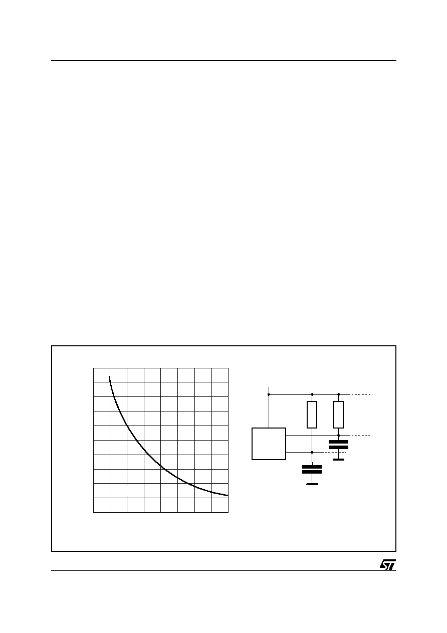
AI01100
VCC
CBUS
SDA
RL
MASTER
RL
SCL
CBUS
100
200
300
400
0
4
8
12
16
20
CBUS (pF)
R
L
max
(k
)
VCC = 5V
Figure 3. Maximum RL Value versus Bus Capacitance (CBUS) for an I2C Bus
The devices with this Write Control feature no
longer support the Multibyte Write mode of opera-
tion, however all other write modes are fully sup-
ported.
Refer to the AN404 Application Note for more de-
tailed information about Write Control feature.
DEVICE OPERATION
I2C Bus Background
The ST24/25x08 support the I2C protocol. This
protocol defines any device that sends data onto
the bus as a transmitter and any device that reads
the data as a receiver. The device that controls the
data transfer is known as the master and the other
as the slave. The master will always initiate a data
transfer and will provide the serial clock for syn-
chronisation. The ST24/25x08 are always slave
devices in all communications.
Start Condition. START is identified by a high to
low transition of the SDA line while the clock SCL
is stable in the high state.A START condition must
precede any command for data transfer. Except
during a programming cycle, the ST24/25x08 con-
tinuously monitor the SDA and SCL signals for a
START condition and will not respond unless one
is given.
Stop Condition. STOP is identified by a low to high
transition of the SDA line while the clock SCL is
stable in the high state. A STOP condition termi-
nates communication between the ST24/25x08
and the bus master. A STOP condition at the end
of a Read command, after and only after a No
Acknowledge, forces the standby state. A STOP
condition at the end of a Write command triggers
the internal EEPROM write cycle.
Acknowledge Bit (ACK). An acknowledge signal
is used to indicate a successfull data transfer. The
bus transmitter, either master or slave, will release
the SDA bus after sending 8 bits of data. During the
9th clock pulse period the receiver pulls the SDA
bus low to acknowledge the receipt of the 8 bits of
data.
Data Input. During data input the ST24/25x08
sample the SDA bus signal on the rising edge of
the clock SCL. Note that for correct device opera-
tion the SDA signal must be stable during the clock
low to high transition and the data must change
ONLY when the SCL line is low.
Memory Addressing. To start communication be-
tween the bus master and the slave ST24/25x08,
the master must initiate a START condition. Follow-
ing this, the master sends onto the SDA bus line 8
bits (MSB first) corresponding to the device select
code (7 bits) and a READ or WRITE bit.
SIGNAL DESCRIPTIONS (cont’d)
4/16
ST24/25C08, ST24/25W08
相关PDF资料 |
PDF描述 |
|---|---|
| ST280C04C1L | 960 A, 400 V, SCR, TO-200AB |
| ST280C04C2L | 960 A, 400 V, SCR, TO-200AB |
| ST280C04C2 | 960 A, 400 V, SCR, TO-200AB |
| ST280C04C3L | 960 A, 400 V, SCR, TO-200AB |
| ST280C04C3 | 960 A, 400 V, SCR, TO-200AB |
相关代理商/技术参数 |
参数描述 |
|---|---|
| ST25C08M1TR | 制造商:STMICROELECTRONICS 制造商全称:STMicroelectronics 功能描述:8 Kbit Serial I2C Bus EEPROM with User-Defined Block Write Protection |
| ST25C08M3 | 制造商:STMICROELECTRONICS 制造商全称:STMicroelectronics 功能描述:I2C Serial EEPROM |
| ST25C08M3TR | 制造商:STMICROELECTRONICS 制造商全称:STMicroelectronics 功能描述:8 Kbit Serial I2C Bus EEPROM with User-Defined Block Write Protection |
| ST25C08M5 | 制造商:STMICROELECTRONICS 制造商全称:STMicroelectronics 功能描述:I2C Serial EEPROM |
| ST25C08M5TR | 制造商:STMICROELECTRONICS 制造商全称:STMicroelectronics 功能描述:8 Kbit Serial I2C Bus EEPROM with User-Defined Block Write Protection |
发布紧急采购,3分钟左右您将得到回复。