- 您现在的位置:买卖IC网 > PDF目录98143 > ST52F510G3B6 (STMICROELECTRONICS) 8-BIT, FLASH, 24 MHz, MICROCONTROLLER, PDIP28 PDF资料下载
参数资料
| 型号: | ST52F510G3B6 |
| 厂商: | STMICROELECTRONICS |
| 元件分类: | 微控制器/微处理器 |
| 英文描述: | 8-BIT, FLASH, 24 MHz, MICROCONTROLLER, PDIP28 |
| 封装: | PLASTIC, DIP-28 |
| 文件页数: | 32/106页 |
| 文件大小: | 1340K |
| 代理商: | ST52F510G3B6 |
第1页第2页第3页第4页第5页第6页第7页第8页第9页第10页第11页第12页第13页第14页第15页第16页第17页第18页第19页第20页第21页第22页第23页第24页第25页第26页第27页第28页第29页第30页第31页当前第32页第33页第34页第35页第36页第37页第38页第39页第40页第41页第42页第43页第44页第45页第46页第47页第48页第49页第50页第51页第52页第53页第54页第55页第56页第57页第58页第59页第60页第61页第62页第63页第64页第65页第66页第67页第68页第69页第70页第71页第72页第73页第74页第75页第76页第77页第78页第79页第80页第81页第82页第83页第84页第85页第86页第87页第88页第89页第90页第91页第92页第93页第94页第95页第96页第97页第98页第99页第100页第101页第102页第103页第104页第105页第106页
31/106
4 MEMORY PROGRAMMING
ST52F510/F513/F514 provides an on-chip user
programmable non-volatile memory, which allows
fast and reliable storage of user data.
Program/Data
Memory
addressing
space
is
composed by a Single Voltage Flash Memory and
a RAM memory bench. The ST52F513/514
devices also have a Data EEPROM bench to store
permanent data with long term retention and a high
number of write/erase cycles.
All the Program Data memory addresses can
execute code, including RAM and EEPROM
benches.
The memory is programmed by setting the Vpp pin
equal to Vdd. Data and commands are transmitted
through the I2C serial communication protocol. The
same procedure is used to perform “In-Situ” the
programming of the device after it is mounted in
the user system. Data can also be written in run-
time with the In-Application Programming (IAP).
The Memory can be locked by the user during the
programming phase, in order to prevent external
operation such as reading the program code and
assuring protection of user intellectual property.
Flash and EEPROM pages can be protected by
unintentional writings.
Remark: the memory contents are protected by
the Error Correction Code (ECC) algorithm that
uses a 4-bit redundancy to correct one bit errors.
Warning: when entering the ISP, the default
values for Option Bytes are considered, so a
Voltage Supply higher than the PLVD lower
threshold must be applied to program the device.
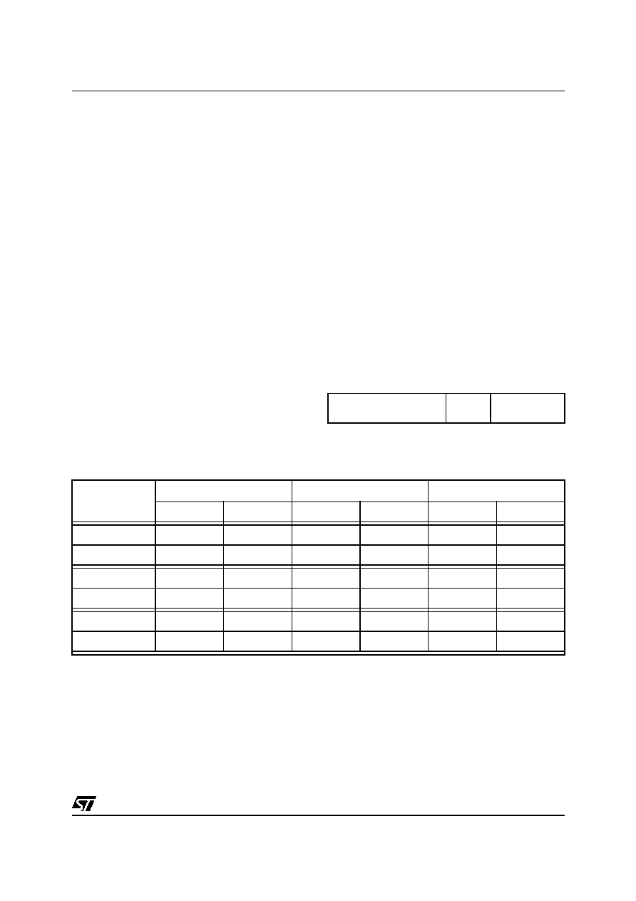
4.1 Program/Data Memory Organization
The Program/Data Memory is organized as
described in Section 3.3. The various sales types
have different amounts of each type of memory.
Table 4.1 describes the memory benches amount
and page allocation for each sales type.
The addressing spaces are organized in pages of
256 bytes. Each page is composed by blocks of 32
bytes. Memory programming is performed one
block at a time in order to speed-up the
programming time (about 2.5 ms per block).
The whole location address is composed as
follows:
15
87
54
0
Page address
Block address address inside the block
Table 4.1 Sales Type Memory Organization
Device
Flash Memory
RAM Memory
EEPROM Memory
Amount
Pages
Amount
Page
Amount
Page(s)
ST52F510c2p6
4096 bytes
0 to 15
256 bytes
32
-
ST52F510c3p6
8192 bytes
0 to 31
256 bytes
32
-
ST52F513c2p6
3840 bytes
0 to 14
256 bytes
32
256 bytes
15
ST52F513c3p6
7936 bytes
0 to 30
256 bytes
32
256 bytes
31
ST52F514c1p6
4096 bytes
0 to 15
256 bytes
32
1024 bytes
16-19
ST52F514c3p6
4096 bytes
0 to 15
256 bytes
32
4096 bytes
16-31
legend:
c:
Y=16 pins, F=20 pins, G=28 pins, K=32/34 pin
p:
B=DIP, M=SO, T=TQFP
相关PDF资料 |
PDF描述 |
|---|---|
| ST52F514G3B6 | 8-BIT, FLASH, 24 MHz, MICROCONTROLLER, PDIP28 |
| ST52F513G3B6 | 8-BIT, FLASH, 24 MHz, MICROCONTROLLER, PDIP28 |
| ST52F513Y1B6 | 8-BIT, FLASH, 24 MHz, MICROCONTROLLER, PDIP16 |
| ST52F513Y2B6 | 8-BIT, FLASH, 24 MHz, MICROCONTROLLER, PDIP16 |
| ST52F510Y3B6 | 8-BIT, FLASH, 24 MHz, MICROCONTROLLER, PDIP16 |
相关代理商/技术参数 |
参数描述 |
|---|---|
| ST52F510GMB6 | 制造商:STMICROELECTRONICS 制造商全称:STMicroelectronics 功能描述:8-BIT INTELLIGENT CONTROLLER UNIT ICU Two Timer/PWMs, ADC, I2C, SPI, SCI |
| ST52F510GMM6 | 制造商:STMICROELECTRONICS 制造商全称:STMicroelectronics 功能描述:8-BIT INTELLIGENT CONTROLLER UNIT ICU Two Timer/PWMs, ADC, I2C, SPI, SCI |
| ST52F510YMM6 | 制造商:STMICROELECTRONICS 制造商全称:STMicroelectronics 功能描述:8-BIT INTELLIGENT CONTROLLER UNIT ICU Two Timer/PWMs, ADC, I2C, SPI, SCI |
| ST52F513 | 制造商:STMICROELECTRONICS 制造商全称:STMicroelectronics 功能描述:8-BIT INTELLIGENT CONTROLLER UNIT ICU Two Timer/PWMs, ADC, I2C, SPI, SCI |
| ST52F513FMB6 | 制造商:STMICROELECTRONICS 制造商全称:STMicroelectronics 功能描述:8-BIT INTELLIGENT CONTROLLER UNIT ICU Two Timer/PWMs, ADC, I2C, SPI, SCI |
发布紧急采购,3分钟左右您将得到回复。