- 您现在的位置:买卖IC网 > PDF目录98144 > ST62P18CB1/XXX (STMICROELECTRONICS) 8-BIT, MROM, 8 MHz, MICROCONTROLLER, PDIP20 PDF资料下载
参数资料
| 型号: | ST62P18CB1/XXX |
| 厂商: | STMICROELECTRONICS |
| 元件分类: | 微控制器/微处理器 |
| 英文描述: | 8-BIT, MROM, 8 MHz, MICROCONTROLLER, PDIP20 |
| 封装: | 0.300 INCH, PLASTIC, DIP-20 |
| 文件页数: | 63/82页 |
| 文件大小: | 937K |
| 代理商: | ST62P18CB1/XXX |
第1页第2页第3页第4页第5页第6页第7页第8页第9页第10页第11页第12页第13页第14页第15页第16页第17页第18页第19页第20页第21页第22页第23页第24页第25页第26页第27页第28页第29页第30页第31页第32页第33页第34页第35页第36页第37页第38页第39页第40页第41页第42页第43页第44页第45页第46页第47页第48页第49页第50页第51页第52页第53页第54页第55页第56页第57页第58页第59页第60页第61页第62页当前第63页第64页第65页第66页第67页第68页第69页第70页第71页第72页第73页第74页第75页第76页第77页第78页第79页第80页第81页第82页
Obsolete
Product(s)
- Obsolete
Product(s)
66/82
ST62T18C/E18C
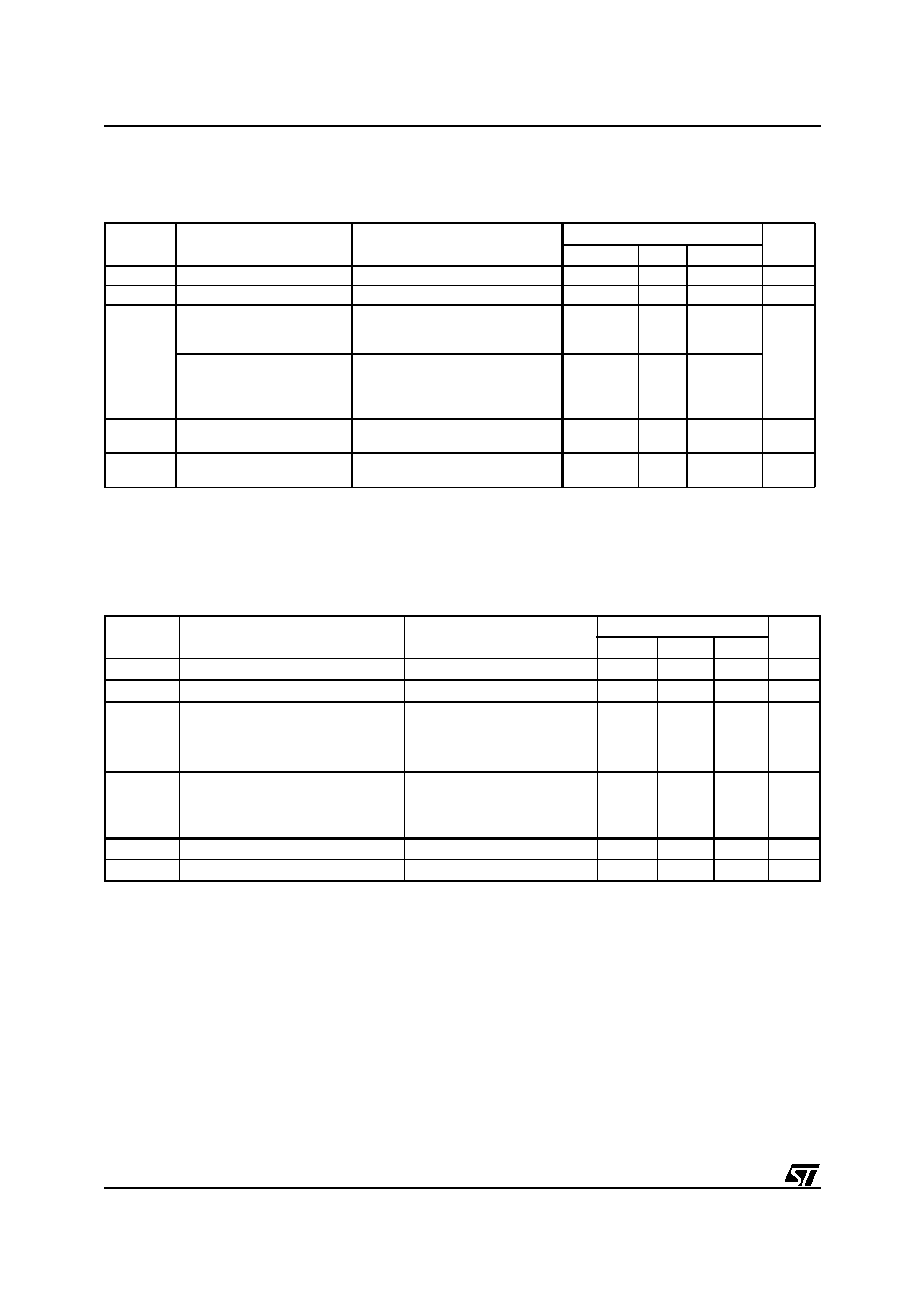
DC ELECTRICAL CHARACTERISTICS (Cont’d)
(TA = -40 to +85°C unless otherwise specified))
Note:
(*) All Peripherals in stand-by.
6.4 AC ELECTRICAL CHARACTERISTICS
(TA = -40 to +125°C unless otherwise specified)
Notes:
1. Period for which VDD has to be connected at 0V to allow internal Reset function at next power-up.
2 An oscillator frequency above 1MHz is recommended for reliable A/D results.
3. Measure performed with OSCin pin soldered on PCB, with an around 2pF equivalent capacitance.
Symbol
Parameter
Test Conditions
Value
Unit
Min.
Typ.
Max.
Vup
LVD Threshold in power-on
Vdn +50 mV
4.1
4.3
V
Vdn
LVD threshold in powerdown
3.6
3.8
Vup -50 mV
V
VOL
Low Level Output Voltage
All Output pins
VDD= 5.0V; IOL = +10A
VDD= 5.0V; IOL = + 5mA
VDD= 5.0V; IOL = + 10mAv
0.1
0.8
1.2
V
Low Level Output Voltage
20 mA Sink I/O pins
VDD= 5.0V; IOL = +10A
VDD= 5.0V; IOL = +10mA
VDD= 5.0V; IOL = +20mA
VDD= 5.0V; IOL = +30mA
0.1
0.8
1.3
2.0
VOH
High Level Output Voltage
All Output pins
VDD= 5.0V; IOH = -10A
VDD= 5.0V; IOH = -5.0mA
4.9
3.5
V
IDD
Supply Current in STOP
Mode, with LVD disabled(*)
ILOAD=0mA
VDD=5.0V
10
A
Symbol
Parameter
Test Conditions
Value
Unit
Min.
Typ.
Max.
tREC
Supply Recovery Time (1)
100
ms
fLFAO
Internal frequency with LFAO active
200
400
800
kHz
fOSG
Internal Frequency with OSG
enabled2)
VDD = 3V
VDD = 3.6V
VDD = 4.5V
VDD = 6V
1
2
fOSC
MHz
fRC
Internal frequency with RC oscillator
and OSG disabled2) 3)
VDD=5.0V
R=47k
R=100k
R=470k
4
2.7
800
5
3.2
850
5.8
3.5
900
MHz
kHz
CIN
Input Capacitance
All Inputs Pins
10
pF
COUT
Output Capacitance
All Outputs Pins
10
pF
66
相关PDF资料 |
PDF描述 |
|---|---|
| ST6327B1 | 8-BIT, MROM, 8 MHz, MICROCONTROLLER, PDIP42 |
| ST6375B1/XXX | 8-BIT, MROM, 8 MHz, MICROCONTROLLER, PDIP42 |
| ST6367B1/XXX | 8-BIT, MROM, 8 MHz, MICROCONTROLLER, PDIP42 |
| ST6382B1/XXX | 8-BIT, MROM, MICROCONTROLLER, PDIP42 |
| ST6386B1 | 8-BIT, MROM, 8 MHz, MICROCONTROLLER, PDIP42 |
相关代理商/技术参数 |
参数描述 |
|---|---|
| ST62P52C | 制造商:STMicroelectronics 功能描述: |
| ST62P62CM6/MOMTR | 制造商:STMicroelectronics 功能描述: |
| ST62P62CM6/MPITR | 制造商:STMicroelectronics 功能描述: |
| ST62P62CM6/MSATR | 制造商:STMicroelectronics 功能描述: |
| ST62P62CN6/MMMTR | 制造商:STMicroelectronics 功能描述: |
发布紧急采购,3分钟左右您将得到回复。