- 您现在的位置:买卖IC网 > PDF目录69350 > ST62P65CB3/XXX (STMICROELECTRONICS) 8-BIT, MROM, 8 MHz, MICROCONTROLLER, PDIP28 PDF资料下载
参数资料
| 型号: | ST62P65CB3/XXX |
| 厂商: | STMICROELECTRONICS |
| 元件分类: | 微控制器/微处理器 |
| 英文描述: | 8-BIT, MROM, 8 MHz, MICROCONTROLLER, PDIP28 |
| 封装: | 0.600 INCH, PLASTIC, DIP-28 |
| 文件页数: | 86/86页 |
| 文件大小: | 970K |
| 代理商: | ST62P65CB3/XXX |
第1页第2页第3页第4页第5页第6页第7页第8页第9页第10页第11页第12页第13页第14页第15页第16页第17页第18页第19页第20页第21页第22页第23页第24页第25页第26页第27页第28页第29页第30页第31页第32页第33页第34页第35页第36页第37页第38页第39页第40页第41页第42页第43页第44页第45页第46页第47页第48页第49页第50页第51页第52页第53页第54页第55页第56页第57页第58页第59页第60页第61页第62页第63页第64页第65页第66页第67页第68页第69页第70页第71页第72页第73页第74页第75页第76页第77页第78页第79页第80页第81页第82页第83页第84页第85页当前第86页
9/86
ST62T55C ST62T65C/E65C
MEMORY MAP (Cont’d)
1.3.3 Data Space
Data Space accommodates all the data necessary
for processing the user program. This space com-
prises the RAM resource, the processor core and
peripheral registers, as well as read-only data
such as constants and look-up tables in OTP/
EPROM.
1.3.3.1 Data ROM
All read-only data is physically stored in program
memory, which also accommodates the Program
Space. The program memory consequently con-
tains the program code to be executed, as well as
the constants and look-up tables required by the
application.
The Data Space locations in which the different
constants and look-up tables are addressed by the
processor core may be thought of as a 64-byte
window through which it is possible to access the
read-only data stored in OTP/EPROM.
1.3.3.2 Data RAM/EEPROM
In ST62T55C, ST62T65C and ST62E65C devic-
es, the data space includes 60 bytes of RAM, the
accumulator (A), the indirect registers (X), (Y), the
short direct registers (V), (W), the I/O port regis-
ters, the peripheral data and control registers, the
interrupt option register and the Data ROM Win-
dow register (DRW register).
Additional RAM and EEPROM pages can also be
addressed using banks of 64 bytes located be-
tween addresses 00h and 3Fh.
1.3.4 Stack Space
Stack space consists of six 12-bit registers which
are used to stack subroutine and interrupt return
addresses, as well as the current program counter
contents.
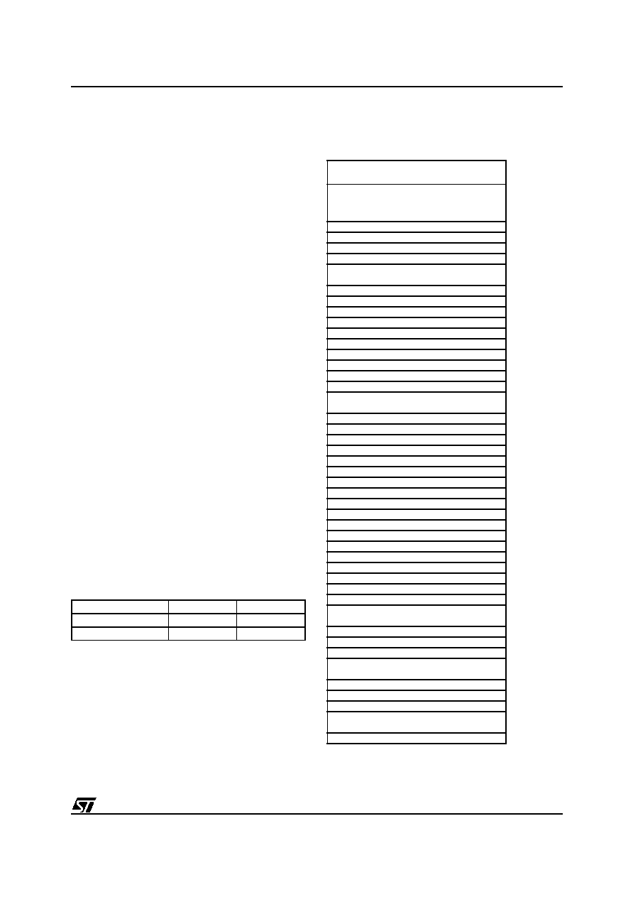
Table 1. Additional RAM/EEPROM Banks
Table 2. ST62T55C, ST62T65C and ST62E65C
Data Memory Space
Device
RAM
EEPROM
ST62T55C
1 x 64 bytes
-
ST62T65C/E65C
1 x 64 bytes
2 x 64 bytes
RAM and EEPROM
000h
03Fh
DATA ROM WINDOW AREA
040h
07Fh
X REGISTER
080h
Y REGISTER
081h
V REGISTER
082h
W REGISTER
083h
DATA RAM 60 BYTES
084h
0BFh
PORT A DATA REGISTER
0C0h
PORT B DATA REGISTER
0C1h
PORT C DATA REGISTER
0C2h
RESERVED
0C3h
PORT A DIRECTION REGISTER
0C4h
PORT B DIRECTION REGISTER
0C5h
PORT C DIRECTION REGISTER
0C6h
RESERVED
0C7h
INTERRUPT OPTION REGISTER
0C8h*
DATA ROM WINDOW REGISTER
0C9h*
RESERVED
0CAh
0CBh
PORT A OPTION REGISTER
0CCh
PORT B OPTION REGISTER
0CDh
PORT C OPTION REGISTER
0CEh
RESERVED
0CFh
A/D DATA REGISTER
0D0h
A/D CONTROL REGISTER
0D1h
TIMER PRESCALER REGISTER
0D2h
TIMER COUNTER REGISTER
0D3h
TIMER STATUS CONTROL REGISTER
0D4h
AR TIMER MODE CONTROL REGISTER
0D5h
AR TIMER STATUS/CONTROL REGISTER1
0D6h
AR TIMER STATUS/CONTROL REGISTER2
0D7h
WATCHDOG REGISTER
0D8h
AR TIMER RELOAD/CAPTURE REGISTER
0D9h
AR TIMER COMPARE REGISTER
0DAh
AR TIMER LOAD REGISTER
0DBh
OSCILLATOR CONTROL REGISTER
0DCh*
MISCELLANEOUS
0DDh
RESERVED
0DEh
0DFh
SPI DATA REGISTER
0E0h
SPI DIVIDER REGISTER
0E1h
SPI MODE REGISTER
0E2h
RESERVED
0E3h
0E7h
DATA RAM/EEPROM REGISTER
0E8h*
RESERVED
0E9h
EEPROM CONTROL REGISTER
0EAh
RESERVED
0EBh
0FEh
ACCUMULATOR
0FFh
* WRITE ONLY REGISTER
相关PDF资料 |
PDF描述 |
|---|---|
| ST62P55CM6/XXX | 8-BIT, MROM, 8 MHz, MICROCONTROLLER, PDSO28 |
| ST62P65CM3/XXX | 8-BIT, MROM, 8 MHz, MICROCONTROLLER, PDSO28 |
| ST62T03CB6 | 8-BIT, OTPROM, 8 MHz, MICROCONTROLLER, PDIP16 |
| ST62T01CB1 | 8-BIT, OTPROM, 8 MHz, MICROCONTROLLER, PDIP16 |
| ST62P00CB3/XXX | 8-BIT, MROM, 8 MHz, MICROCONTROLLER, PDIP16 |
相关代理商/技术参数 |
参数描述 |
|---|---|
| ST62P65CM6/MRYTR | 制造商:STMicroelectronics 功能描述: |
| ST62P65CM6/RAL/TR | 制造商:STMicroelectronics 功能描述: |
| ST62P65CM6/RAP/TR | 制造商:STMicroelectronics 功能描述: |
| ST62T00CB6 | 功能描述:8位微控制器 -MCU OTP EPROM 1K No Intf RoHS:否 制造商:Silicon Labs 核心:8051 处理器系列:C8051F39x 数据总线宽度:8 bit 最大时钟频率:50 MHz 程序存储器大小:16 KB 数据 RAM 大小:1 KB 片上 ADC:Yes 工作电源电压:1.8 V to 3.6 V 工作温度范围:- 40 C to + 105 C 封装 / 箱体:QFN-20 安装风格:SMD/SMT |
| ST62T00CB6 | 制造商:STMicroelectronics 功能描述:IC 8BIT MCU OTP 1K 62T00 DIP16 |
发布紧急采购,3分钟左右您将得到回复。