- 您现在的位置:买卖IC网 > PDF目录385870 > ST62T40B (意法半导体) The CAT24FC02 is a 2-kb Serial CMOS EEPROM internally organized as 256 words of 8 bits each PDF资料下载
参数资料
| 型号: | ST62T40B |
| 厂商: | 意法半导体 |
| 元件分类: | DRAM |
| 英文描述: | The CAT24FC02 is a 2-kb Serial CMOS EEPROM internally organized as 256 words of 8 bits each |
| 中文描述: | 该CAT24FC02是一个2 KB的EEPROM的国内256个8位每字举办的串行CMOS |
| 文件页数: | 12/72页 |
| 文件大小: | 445K |
| 代理商: | ST62T40B |
第1页第2页第3页第4页第5页第6页第7页第8页第9页第10页第11页当前第12页第13页第14页第15页第16页第17页第18页第19页第20页第21页第22页第23页第24页第25页第26页第27页第28页第29页第30页第31页第32页第33页第34页第35页第36页第37页第38页第39页第40页第41页第42页第43页第44页第45页第46页第47页第48页第49页第50页第51页第52页第53页第54页第55页第56页第57页第58页第59页第60页第61页第62页第63页第64页第65页第66页第67页第68页第69页第70页第71页第72页
12/72
12
ST62T40B/E40B
MEMORY MAP
(Cont’d)
1.3.6
Data
(DRBR)
Address: CBh
RAM/EEPROM
Bank
Register
—
Write only
Bit 7-5 = These bits are not used
Bit 4 -
DRBR4
. This bit, when set, selects RAM
Page 2.
Bit 3 -
DRBR3
. This bit, when set, selects RAM
Page 1.
Bit2. These bits are not used.
Bit 1 -
DRBR1
. This bit, when set, selects
EEPROM Page 1.
Bit 0 -
DRBR0
. This bit, when set, selects
EEPROM Page 0.
The selection of the bankis madeby programming
the Data RAM Bank Switch register (DRBR regis-
ter) located at address CBh of the Data Space ac-
cording to Table 1. No more than one bank should
be set at a time.
The DRBR register can be addressed like a RAM
Data Space at the address CBh; nevertheless it is
a write only register that cannot be accessed with
single-bit operations.This register is used to select
the desired 64-byte RAM/EEPROM bank of the
Data Space. The number of banks has to be load-
ed in the DRBR register and the instruction has to
point to the selected location as if it was in bank 0
(from 00h address to 3Fh address).
This register is not cleared during the MCU initiali-
zation, therefore it must be written before the first
access to the Data Space bank region. Refer to
the Data Space description for additional informa-
tion. The DRBR register is not modified when an
interrupt or a subroutine occurs.
Notes
:
Care is required when handling the DRBR register
as it is write only. For this reason, it is not allowed
to change the DRBR contents while executing in-
terrupt service routine, as the service routine can-
not save and then restore its previous content. If it
is impossible to avoid the writing of this register in
interrupt service routine, an image of this register
must be saved in a RAM location, and each time
the program writes to DRBR it must write also to
the image register. The image register must be
written first, so if an interrupt occurs between the
two instructions the DRBR is not affected.
In DRBR Register, only 1 bit must be set. Other-
wise two or more pages are enabled in parallel,
producing errors.
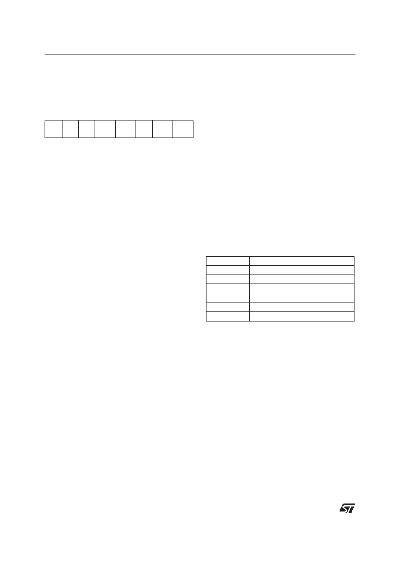
Table 6. Data RAM Bank Register Set-up
7
0
-
-
-
DRBR4 DRBR3
-
DRBR1 DRBR0
DRBR
00h
01h
02h
08h
10h
other
ST62T40B/E40B
None
EEPROM Page 0
EEPROM Page 1
RAM Page 1
RAM Page 2
Reserved
相关PDF资料 |
PDF描述 |
|---|---|
| ST62T10 | 8-BIT OTP/EPROM MCUs WITH A/D CONVERTER |
| ST62T28C | 8-BIT MCUs WITH A/D CONVERTER, AUTO-RELOAD TIMER, UART, OSG, SAFE RESET AND 28-PIN PACKAGE |
| ST6228CN1 | ER 3C 3#16S SKT RECP WALL |
| ST6228CN3 | CB 5C 5#16S PIN RECP WALL |
| ST6228CN6 | ER 5C 5#16S PIN RECP WALL |
相关代理商/技术参数 |
参数描述 |
|---|---|
| ST62T40BQ6 | 功能描述:8位微控制器 -MCU OTP EPROM 8K SPI RoHS:否 制造商:Silicon Labs 核心:8051 处理器系列:C8051F39x 数据总线宽度:8 bit 最大时钟频率:50 MHz 程序存储器大小:16 KB 数据 RAM 大小:1 KB 片上 ADC:Yes 工作电源电压:1.8 V to 3.6 V 工作温度范围:- 40 C to + 105 C 封装 / 箱体:QFN-20 安装风格:SMD/SMT |
| ST62T42BQ6 | 功能描述:8位微控制器 -MCU OTP EPROM 8K SPI RoHS:否 制造商:Silicon Labs 核心:8051 处理器系列:C8051F39x 数据总线宽度:8 bit 最大时钟频率:50 MHz 程序存储器大小:16 KB 数据 RAM 大小:1 KB 片上 ADC:Yes 工作电源电压:1.8 V to 3.6 V 工作温度范围:- 40 C to + 105 C 封装 / 箱体:QFN-20 安装风格:SMD/SMT |
| ST62T45BQ6 | 功能描述:8位微控制器 -MCU OTP EPROM 8K RoHS:否 制造商:Silicon Labs 核心:8051 处理器系列:C8051F39x 数据总线宽度:8 bit 最大时钟频率:50 MHz 程序存储器大小:16 KB 数据 RAM 大小:1 KB 片上 ADC:Yes 工作电源电压:1.8 V to 3.6 V 工作温度范围:- 40 C to + 105 C 封装 / 箱体:QFN-20 安装风格:SMD/SMT |
| ST62T45Q6 | 制造商:STMicroelectronics 功能描述:8BIT MCU - Bulk |
| ST62T46BB6 | 功能描述:8位微控制器 -MCU OTP EPROM 4K SPI RoHS:否 制造商:Silicon Labs 核心:8051 处理器系列:C8051F39x 数据总线宽度:8 bit 最大时钟频率:50 MHz 程序存储器大小:16 KB 数据 RAM 大小:1 KB 片上 ADC:Yes 工作电源电压:1.8 V to 3.6 V 工作温度范围:- 40 C to + 105 C 封装 / 箱体:QFN-20 安装风格:SMD/SMT |
发布紧急采购,3分钟左右您将得到回复。